特性
- Low voltage single supply operation: VDD = 2.5V to 5.5V
- Low input offset voltage: VIO ≤ ±6.0mV
- Low input bias current: IB ≤ (1pA).
- Wide output voltage range: VOUT : VSS+0.1V to VDD-0.1V(@Io=5mA)
- Supply current (per channel): IDD = 0.75mA Typ.
- High slew rate: SR = 8V/μs Typ. ( ) reference value of design
描述
The READ2302G is input and output full range dual CMOS Operational Amplifier realizing high drivability and high slew rate. This IC can be used in minimum operating supply voltage from 2. 5V, and in wide ambient temperature range from -40°C to +105°C. Available in ultra-small 8 pins TSSOP packages.
| Part Number | Status | Samples | Stock | RoHS | Package | Budgetary Price (USD) | Lead Count (#) | Moisture Sensitivity Level (MSL) | Pb (Lead) Free | Country of Assembly | Country of Wafer Fabrication |
|---|---|---|---|---|---|---|---|---|---|---|---|
| READ2302GSP#GC0 | Obsolete | N/A | Out of Stock | RoHS:EN RoHS:JA | TSSOP | 8# | Yes | ||||
| READ2302GSP#GC3 | Obsolete | Available | In Stock | Contact | TSSOP | 1ku | $0.484 | 8# | 1 | Yes | MALAYSIA | JAPAN |
- 白皮书英语Single Stage Microinverter Topology: A Full System Design Solution for Both On/Off-Grid ApplicationsPDF 441 KB 2025年7月01日Microinverters using Gallium Nitride (GaN) switches offer compact, high-efficiency solutions for solar energy systems. This paper presents a single-stage design that delivers up to 500W with low total harmonic distortion and high power density, supporting both grid-tied and off-grid loads.
- 应用说明英语PDF 263 KB r13an0003eu0100-biasing-op-amps 2019年12月06日AI 生成的摘要: Proper biasing of operational amplifiers is essential to avoid malfunction in AC-coupled circuits. A missing DC bias path causes long stabilization times and potential failures. Adding input resistors to ground provides a DC path for bias currents, minimizing offset errors. For single-supply AC-coupled amplifiers, biasing uses a reference voltage, ideally from a high-PSRR voltage reference or buffered voltage divider, to maintain signal symmetry and reduce noise. Understanding frequency responses of input and feedback components is crucial for setting bandwidth and gain characteristics.
- 应用说明英语PDF 206 KB r13an0002eu-composite-amplifier 2019年9月09日AI 生成的摘要: The document details the design of a composite amplifier using ISL28134 and READ2302 for high gain applications. It derives key parameters like unity gain bandwidth, showing the composite amplifier achieves 4.58MHz. It explains phase compensation using a capacitor for either maximum bandwidth or maximum phase margin, providing equations and practical component values. The composite amplifier significantly extends signal bandwidth compared to a standard amplifier, increasing it up to seven times for maximum bandwidth and nearly three times for maximum phase margin.
- 应用说明英语PDF 564 KB an1993 2018年5月22日AI 生成的摘要: Voltage feedback (VFB) amplifiers use a differential input pair, a high-impedance stage, and an output buffer to convert input voltage differences into output voltage. The VFB amplifier's gain decreases at a dominant pole frequency due to compensation capacitors. Current feedback (CFB) amplifiers include a class AB input amplifier, current mirror, high-impedance stage, and output buffer. CFB amplifiers provide faster switching and higher slew rates by drawing charge/discharge currents directly from supply rails, unlike VFB amplifiers which are limited by biasing current sources.
- 应用说明英语PDF 357 KB an1694 2004年1月19日AI 生成的摘要: The document outlines the four fundamental internal blocks of an operational amplifier and presents a simple 2:1 stage circuit diagram. It includes important legal notices from Renesas Electronics regarding the use, liability, and intellectual property rights of their semiconductor products. The document clarifies product quality grades, intended applications, and restrictions on use in life-critical or hazardous systems. It emphasizes compliance with applicable laws and safety responsibilities when using Renesas products. Contact information for Renesas sales offices worldwide is also provided.
推荐文档 (1)
数据手册 (1)
No Results Found.
确保所有关键词拼写正确。
尝试使用更少、不同或更宽泛的词语来改变搜索结果。
如果您使用了筛选器,请考虑取消选择某些筛选器选项以扩大搜索结果。
- 搜索我们丰富的知识库,帮助您解答常见问题
- 前往支持论坛,获取瑞萨电子技术专家和社群的帮助
- 白皮书英语Single Stage Microinverter Topology: A Full System Design Solution for Both On/Off-Grid ApplicationsPDF 441 KB 2025年7月01日Microinverters using Gallium Nitride (GaN) switches offer compact, high-efficiency solutions for solar energy systems. This paper presents a single-stage design that delivers up to 500W with low total harmonic distortion and high power density, supporting both grid-tied and off-grid loads.
- 应用说明英语PDF 263 KB r13an0003eu0100-biasing-op-amps 2019年12月06日AI 生成的摘要: Proper biasing of operational amplifiers is essential to avoid malfunction in AC-coupled circuits. A missing DC bias path causes long stabilization times and potential failures. Adding input resistors to ground provides a DC path for bias currents, minimizing offset errors. For single-supply AC-coupled amplifiers, biasing uses a reference voltage, ideally from a high-PSRR voltage reference or buffered voltage divider, to maintain signal symmetry and reduce noise. Understanding frequency responses of input and feedback components is crucial for setting bandwidth and gain characteristics.
- 应用说明英语PDF 206 KB r13an0002eu-composite-amplifier 2019年9月09日AI 生成的摘要: The document details the design of a composite amplifier using ISL28134 and READ2302 for high gain applications. It derives key parameters like unity gain bandwidth, showing the composite amplifier achieves 4.58MHz. It explains phase compensation using a capacitor for either maximum bandwidth or maximum phase margin, providing equations and practical component values. The composite amplifier significantly extends signal bandwidth compared to a standard amplifier, increasing it up to seven times for maximum bandwidth and nearly three times for maximum phase margin.
- 应用说明英语PDF 564 KB an1993 2018年5月22日AI 生成的摘要: Voltage feedback (VFB) amplifiers use a differential input pair, a high-impedance stage, and an output buffer to convert input voltage differences into output voltage. The VFB amplifier's gain decreases at a dominant pole frequency due to compensation capacitors. Current feedback (CFB) amplifiers include a class AB input amplifier, current mirror, high-impedance stage, and output buffer. CFB amplifiers provide faster switching and higher slew rates by drawing charge/discharge currents directly from supply rails, unlike VFB amplifiers which are limited by biasing current sources.
- 应用说明英语PDF 357 KB an1694 2004年1月19日AI 生成的摘要: The document outlines the four fundamental internal blocks of an operational amplifier and presents a simple 2:1 stage circuit diagram. It includes important legal notices from Renesas Electronics regarding the use, liability, and intellectual property rights of their semiconductor products. The document clarifies product quality grades, intended applications, and restrictions on use in life-critical or hazardous systems. It emphasizes compliance with applicable laws and safety responsibilities when using Renesas products. Contact information for Renesas sales offices worldwide is also provided.
应用说明和白皮书 (5)
No Results Found.
确保所有关键词拼写正确。
尝试使用更少、不同或更宽泛的词语来改变搜索结果。
如果您使用了筛选器,请考虑取消选择某些筛选器选项以扩大搜索结果。
- 搜索我们丰富的知识库,帮助您解答常见问题
- 前往支持论坛,获取瑞萨电子技术专家和社群的帮助
No Results Found.
确保所有关键词拼写正确。
尝试使用更少、不同或更宽泛的词语来改变搜索结果。
如果您使用了筛选器,请考虑取消选择某些筛选器选项以扩大搜索结果。
- 搜索我们丰富的知识库,帮助您解答常见问题
- 前往支持论坛,获取瑞萨电子技术专家和社群的帮助
No Results Found.
确保所有关键词拼写正确。
尝试使用更少、不同或更宽泛的词语来改变搜索结果。
如果您使用了筛选器,请考虑取消选择某些筛选器选项以扩大搜索结果。
- 搜索我们丰富的知识库,帮助您解答常见问题
- 前往支持论坛,获取瑞萨电子技术专家和社群的帮助
No Results Found.
确保所有关键词拼写正确。
尝试使用更少、不同或更宽泛的词语来改变搜索结果。
如果您使用了筛选器,请考虑取消选择某些筛选器选项以扩大搜索结果。
- 搜索我们丰富的知识库,帮助您解答常见问题
- 前往支持论坛,获取瑞萨电子技术专家和社群的帮助
No Results Found.
确保所有关键词拼写正确。
尝试使用更少、不同或更宽泛的词语来改变搜索结果。
如果您使用了筛选器,请考虑取消选择某些筛选器选项以扩大搜索结果。
- 搜索我们丰富的知识库,帮助您解答常见问题
- 前往支持论坛,获取瑞萨电子技术专家和社群的帮助
质量和可靠性 (1)
No Results Found.
确保所有关键词拼写正确。
尝试使用更少、不同或更宽泛的词语来改变搜索结果。
如果您使用了筛选器,请考虑取消选择某些筛选器选项以扩大搜索结果。
- 搜索我们丰富的知识库,帮助您解答常见问题
- 前往支持论坛,获取瑞萨电子技术专家和社群的帮助
营销资料 (1)
No Results Found.
确保所有关键词拼写正确。
尝试使用更少、不同或更宽泛的词语来改变搜索结果。
如果您使用了筛选器,请考虑取消选择某些筛选器选项以扩大搜索结果。
- 搜索我们丰富的知识库,帮助您解答常见问题
- 前往支持论坛,获取瑞萨电子技术专家和社群的帮助
No Results Found.
确保所有关键词拼写正确。
尝试使用更少、不同或更宽泛的词语来改变搜索结果。
如果您使用了筛选器,请考虑取消选择某些筛选器选项以扩大搜索结果。
- 搜索我们丰富的知识库,帮助您解答常见问题
- 前往支持论坛,获取瑞萨电子技术专家和社群的帮助
No Results Found.
确保所有关键词拼写正确。
尝试使用更少、不同或更宽泛的词语来改变搜索结果。
如果您使用了筛选器,请考虑取消选择某些筛选器选项以扩大搜索结果。
- 搜索我们丰富的知识库,帮助您解答常见问题
- 前往支持论坛,获取瑞萨电子技术专家和社群的帮助
Renesas Boards & Kits
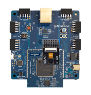
基于 RA6M3 的 AI 套件开发平台
连接功能多种多样,并且可重新配置,助力 AI/ML 系统提速。 硬件平台便捷易用,适用于以 RA 系列 32 位 MCU 中 RA6M3 MCU 为基础的多模态 AI/ML 解决方案。
该硬件平台旨在用于支持实时分析的各种 AI/ML 单/多模态使用场景。 它允许用户将不同的插件式传感器与板载的模拟麦克风、摄像头进行灵活多样的组合。
它由已搭载的 Reality AI 软件提供实时分析支持,此外,针对特定用户场景也可由 Renesas 完善的合作伙伴网络提供方案支持。
AI 套件不仅让您能够评估和测试现有已开发好的应用示例,还可利用现有的生态伙伴和 AI/ML 软件来开发自己的解决方案。
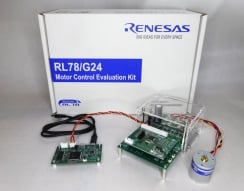
RL78/G24 Motor Control Evaluation Kit
RL78/G24 电机控制评估套件是一款永磁同步电机(无刷直流电机)控制评估套件,配备 RL78/G24 微控制器,可轻松评估电机控制。 您可以从瑞萨电子网站下载示例软件,使用该软件就可以立即开始评估电机控制。
包含硬件套件
- 逆变器板(RTK0EMGPLVB00000BJ)
- RL78/G24 CPU 卡(RTK0EMG240C00000BJ)
- 通信板(RTK0EMXC90Z00000BJ)
- 永磁同步电机(TG-55L-KA)
- 各种电缆、螺丝、垫片
知识库
-
板上提供了哪些类型的麦克风?
每个 VOICE 语音套件提供最多 2 个模拟麦克风和最多 1 个数字麦克风。
2022年6月28日 -
RA4E1 和 RA6E1 微控制器似乎原本不支持 I2S 接口,如何连接数字麦克风?
I2S 是通过在 RA MCU 上使用 SPI 和计时器外设的组合来模拟的。
2022年6月28日 -
是否需要使用外部 USB-UART 转换器与微控制器通信?
不需要,VOICE 套件上的 J-Link OB 芯片提供 USB 转 UART 功能以及标准 J-Link 调试功能。
2022年6月28日