特性
- 逻辑和混合信号电路
- 高度灵活的宏单元
- 回读保护(Read Lock)
- 1.8V (±5%) 至 5V (±10%) VDD
- 1.8V(±5%)至 5V(±10%)VDD2(VDD2 ≤ VDD)
- 工作温度范围:-40°C 至 85°C
- 符合 RoHS 标准/无卤素
- 宏单元总览
- 3 个模拟比较器 (ACMP)
- 19 个组合功能宏单元
- 三个可选的 DFF/锁存器或 2 位 LUT
- 1 个可选的连续 DFF/锁存器或 3 位 LUT
- 4 个可选的 DFF/锁存器或 3 位 LUT
- 1 个可选管道延迟或 3 位 LUT
- 1 个可选可编程函数发生器或 2 位 LUT
- 5 个 8 位延迟/计数器或 3 位 LUT
- 2 个 16 位延迟/计数器或 4 位 LUT
- 2 个带边缘检测器的去毛刺滤波器
- 异步状态机
- 8 状态
- 来自状态转换的灵活输入逻辑
- 串行通信
- 符合 I2C 协议
- 管道延迟 – 16 级/3 路输出(组合功能宏单元的一部分)
- 可编程延迟
- 一个逆变器
- 两个振荡器 (OSC)
- 可配置 25kHz/2MHz
- 25MHz RC 振荡器
- 晶体振荡器
- 上电复位 (POR)
- 8 字节 RAM + OTP 用户存储器
- 可通过 I2C 读取和写的 RAM 内存空间
- 从 OTP 传输的用户定义初始值

描述
SLG46535 提供一个小型低功耗组件来实现常用的混合信号功能。 用户通过对一次性可编程 (OTP) 非易失性存储器 (NVM) 进行编程来配置 SLG46535 的互连逻辑、IO 引脚和宏单元,从而进行电路设计。 这款高灵活性的器件能在超小尺寸、超低功耗的单个集成电路中实现丰富多样的混合信号功能设计。 SLG46535 上的附加电源 (VDD2) 能够在同一设计中连接两个独立的电压域。 用户可将每个电源的专用引脚配置为 VDD 和 VDD2 电压域的输入、输出或输入和输出(由内部逻辑动态控制)。 设计人员可利用现有的宏单元来实现混合信号功能,将两个电压域以高到低和低到高的方向进行简单的直通式电平转换。
产品参数
| 属性 | 值 |
|---|---|
| Nominal VDD | 1.71 - 5.5 |
| VDD2 (V) | 1.71 - 5.5 |
| GPIOs (#) | 11 |
| Special Features | ASM (8 states) |
| ACMP Channels (#) | 3 |
| CNT/DLY (Max) (#) | 7 |
| LUTs (Max) (#) | 17 |
| D Flip-flops (DFFs) (#) | 8 |
| Pipe Delay | 16-stage |
| # of Programable Delays (#) | 1 |
| Oscillator Type | Conf. OSC, Ring OSC, Crystal OSC |
| Interface | I2C |
| Memory Type | OTP |
| Temp. Range (°C) | -40 to +85°C |
封装选项
| Pkg. Type | Pkg. Dimensions (mm) | Lead Count (#) | Pitch (mm) |
|---|---|---|---|
| TQFN | 2.0 x 2.2 | 14 | 0.4 |
应用方框图
 | 无线车载远程信息处理单元 先进的远程信息处理系统可实现无缝连接、NFC 集成、OTA 升级和能源效率。 |
其他应用
- 个人计算机和服务器
- 电脑周边设备
- 消费电子
- 数据通信设备
- 手持式和便携式电子产品
完成您的设计
寻找相关的产品,完善您的设计
Renesas Boards & Kits
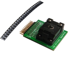
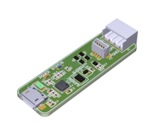
带插座适配器的 GreenPAK SLG46535 开发套件
SLG46535V-SKT 是一款插座适配器套件,可与 SLG4DVKADV GreenPAK™ Advanced 开发板或 SLG4DVKLITE GreenPAK Lite 开发板配套使用。 SLG46535V-SKT 包含 SLG4SA14DS-20x22 插座适配器和 50 个 SLG46535V GreenPAK 可编程混合信号矩阵 IC 样品。
GreenPAK Advanced 开发板和 Lite 开发板与 SLG46xxxX-SKT 和 SLG47xxxV-SKT 插座套件配合使用,为 GreenPAK 器件提供完整的编程、仿真和测试功能。
具有异步状态机和双电源的... 阅读详情
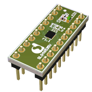
GreenPAK SLG46535 20 引脚 DIP 原型开发板
SLG46535V-DIP 20 引脚 DIP 原型开发板非常适合用于借助 SLG46535 可编程混合信号矩阵 IC(带异步状态机和双电源)进行的模拟板试验和快速原型开发。 它需要 SLG4SA-DIP DIP 适配器才能与 Advanced 开发板配合使用。
GreenPAK™ DIP 适配器是一种小型 PCB,可将 STQFN 封装调整为 DIP 引脚布局。 这款 0.43 英寸 x 1.03 英寸的小型电路板使用 20 引脚 DIP 引脚布局,宽度为 0.3 英寸。 通过使 STQFN 封装与无焊料模拟板兼容,用户还可将此适配器用于原型开发。
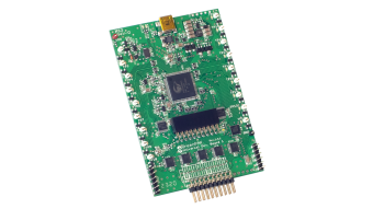
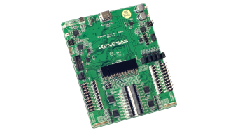
GreenPAK 高级开发板
GreenPAK™ 高级开发板为 GreenPAK 器件提供完整的编程、仿真和测试功能 - 适用于 SLG46xxxX-SKT / SLG47xxxV-SKT 插座套件。
它与 GreenPAK Designer 软件(内置于 Go Configure™ Software Hub 中)协同工作,并允许设计人员: 快速对自定义样品进行编程、 在线测试GreenPAK项目、 和使用任 一 GreenPAK 器件进行开发。
请注意:插座适配器应单独订购
远程测试该板卡
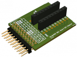
用于 GreenPAK 高级开发板的 GreenPAK DIP 适配器
借助用于 GreenPAK™ 高级开发板的 GreenPAK DIP 适配器,可以将 SLG46xxxV-DIP 和 SLG47xxxV-DIP 原型开发板与 GreenPAK 高级开发板配合使用。 此器件是高级开发平台和 DIP 开发平台之间的桥梁。
GreenPAK 串行调试器板 (GSD)
GreenPAK™ 串行调试器 (GSD) 器件可用于对带有多次可编程非易失性存储器 (NVM) 的 GreenPAK 可编程混合信号矩阵 IC 产品进行编程,或用于配置所有带有 I²C 接口的 GreenPAK 芯片的互连逻辑、IO 和宏单元。 此器件在开发后期阶段非常有用,因为在此阶段,在板上进行调试是最简便的方式。
GSD 适用于 6.xx 及以上版本的 GreenPAK Designer。 在“开发平台选择器”(Development Platform Selector) 窗口中选择 GSD,然后单击“编程或仿真”(Program or Emulate) 按钮。 GSD... 阅读详情
GreenPAK Lite 开发板
GreenPAK Lite 开发板为 GreenPAK 设备提供完整的编程、仿真和测试功能,与 Go Configure™ 软件中心配对工作。 板卡功能由瑞萨电子的 RX66T MCU 提供。


