特性
- High-performance nFET Design
- Low Typical RDSON: 17.6mΩ
- Steady-state Operating Current: 1A
- Low, Fixed Inrush Current: 9mA
- Very Low Supply current after startup: < 1μA
- Operating VDD Range: 2.7V ≤ VDD ≤ 3.6V
- Operating VIN Range: 0.25V ≤ VIN ≤ 1.5V
- Fast VOUT Discharge
- ON/OFF Control: Active HIGH
- Operating Temperature: -40 °C to 85 °C
- Pb-free/Halogen-free/RoHS compliant

描述
The SLG59M1746C is a high-performance 1A capable, single-channel load switch designed for high-side power control applications up to 1A. This feature-rich nFET load switch has been optimized for all small form factor, single-cell Li-ion applications including smartphones, fitness bands, and watches.
Operating from 2.7V to 3.6V supplies, the SLG59M1746C’s RDSON is 17.6mΩ and exhibits an input voltage range that extends from 0.25V to 1.5V. The SLG59M1746C’s nFET architecture achieves very low supply current operation, controlled VIN inrush current profile, and world-class VIN range to rival the performance of many general-purpose nFET and pFET load switches on the market.
Using Renesas’ proprietary MOSFET IP, the SLG59M1746C achieves a stable RDSON as a function of both the supply and input voltages. Fully specified over the -40 °C to 85 °C temperature range, this advanced nFET load switch is available in a 6-lead WLCSP package measuring 0.71mm x 1.16mm x 0.5 mm with 0.35 mm pitch. The SLG59M1746C consumes less than 1μA after start up.
产品参数
| 属性 | 值 |
|---|---|
| FET Pass Device Type | Single N-Channel |
| VDD min. (V) | 2.7 |
| VDD max. (V) | 3.6 |
| VIN Channel 1 min. (V) | 0.25 |
| VIN Channel 1 max. (V) | 1.5 |
| Input Quiescent Current Channel 1, typ (µA) | 15.7 |
| Input Quiescent Current Channel 1, max (µA) | 21.5 |
| Input Quiescent Current when OFF Channel 1, max (µA) | 0.33 |
| RDSON (Typ) Channel 1 (mΩ) | 17.6 |
| IDS Channel 1 (A) | 1 |
| Enable | Active High |
| Output Voltage Slew Rate set by | Internally Fixed |
| Discharge Circuit | Yes |
| Undervoltage Protection | No |
| Over Voltage Protection | No |
| Power Good (PG), FAULT indicator | No |
| Reverse current blocking | No |
| Reverse voltage detection | No |
| Over Current Protection (OCP) | No |
| Short Circuit Protection | No |
| Over Temperature Protection (OTP) | No |
| Current Monitor Output | No |
| Internal TVS Surge Protection | No |
| Temp. Range (°C) | -40 to +85°C |
应用
- Smartphones
- Fitness Bands
- Watches
- Tablet PCs
- GPS Devices
- Portable POS Terminals
Renesas Boards & Kits
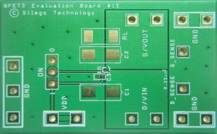
SLG59M1746C Evaluation Board
The SLG59M1746C-EVB board evaluates the SLG59M1746C GreenFET, Single N-Channel, Load Switch.
For details on how to use the evaluation board, please refer to the evaluation board user manual included in the datasheet.


