概览
描述
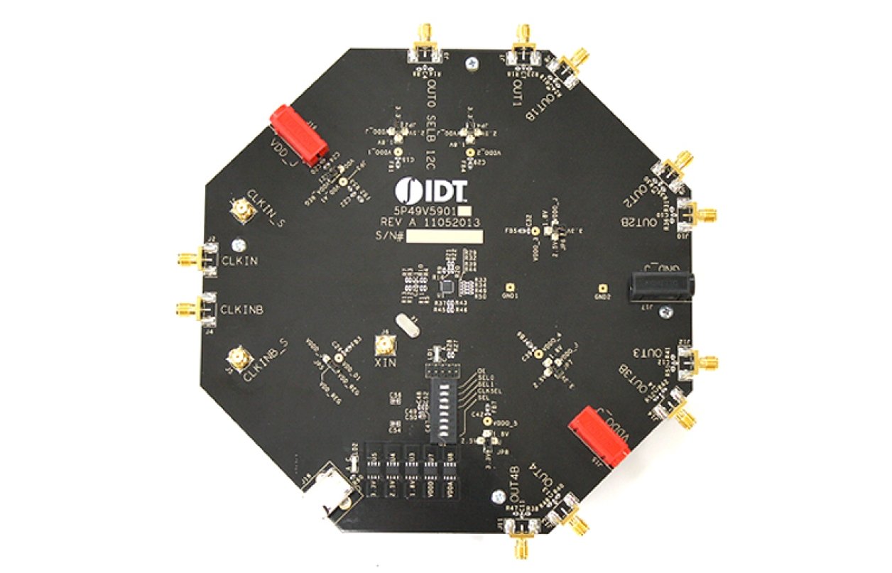
Renesas 5P1105 Programmable buffer outputs can be individually programmed as LVDS, LVPECL, HCSL, or two LVCMOS outputs per output pair, with a crystal, LVCMOS, or differential input. There are up to four universal output pairs, as well as an LVCMOS output clock. Output frequencies range from 1 MHz to 200 MHz for LVCMOS and 1MHz to 35MHz for differential outputs. Output voltage can be individually selected (1.8V, 2.5V, or 3.3V) for each output pair. 5P1105 has four universal outputs and an LVCMOS output. The evaluation board is designed to help the evaluate the 5P1105, the latest addition to the family of programmable devices in Renesas's Timing portfolio.
特性
- 4 Differential Outputs capable of generating any output frequency using Renesas Timing CommanderTM software
- SMA connectors for outputs
- When the board is connected to a PC running Renesas Timing CommanderTM software through USB, the device can be individually programmed as LVDS, LVPECL, HCSL, or two LVCMOS outputs per output pair
- 5P1105 has four universal outputs and an LVCMOS output.
应用
视频和培训
This video introduces the 5P1103 and 5P1105 Programmable Fanout Buffers, emphasizing their performance and flexibility. The video delves into their size, cost, and power efficiency, presenting a comprehensive analysis of these features.


