特性
- High-performance 1:6 LVCMOS clock buffer
- Very low pin-to-pin skew: < 50ps
- Very low additive jitter: < 50fs
- Supply voltage: 1.8V to 3.3V
- fMAX = 200MHz
- Integrated serial termination for 50Ω channel
- Packaged in 14-pin TSSOP and small 16-pin QFN packages
- Extended (-40 °C to +105 °C) temperature range


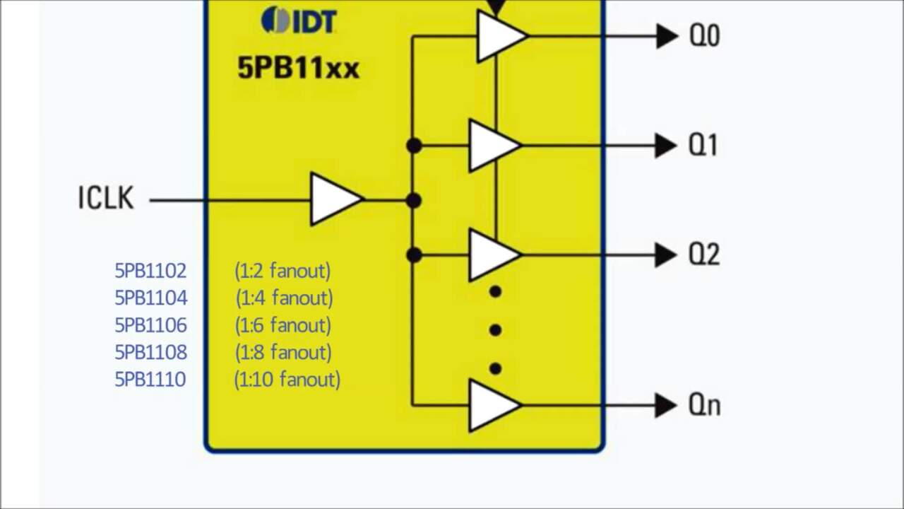
5PB11xx Block Diagram
描述
The 5PB1106 is a high-performance 1:6 LVCMOS clock buffer that offers a best-in-class additive phase jitter of 50fs RMS. This clock buffer also supports an Output Enable function. It is available in 16-pin QFN and 14-pin TSSOP packages and can operate from a 1.8V to 3.3V supply.
产品参数
| 属性 | 值 |
|---|---|
| Temp. Range (°C) | -40 to 85°C, -40 to 105°C |
| Product Category | Clock Buffers & Drivers |
应用
- Industrial applications
- Automotive Radar, LiDAR, and other applications
| Part Number | Status | Samples | Longevity | Stock | Package | Budgetary Price (USD) | Lead Count (#) | Carrier Type | Moisture Sensitivity Level (MSL) | Qty. per Reel (#) | Package Area (mm²) | Pitch (mm) | Pkg. Dimensions (mm) | Reel Size (in) | Qty. per Carrier (#) | Pb (Lead) Free | Pb Free Category | Temp. Range (°C) | Country of Assembly | Country of Wafer Fabrication |
|---|---|---|---|---|---|---|---|---|---|---|---|---|---|---|---|---|---|---|---|---|
| 5PB1106CMGI | Active | Available | 2040 Apr | In Stock | COL | 1ku | $1.19 | 16# | Cut Tape | 1 | 4000# | 6.3mm² | 0.4mm | 2.5 x 2.5 x 0.5 | 7in | 0 | Yes | e3 Sn | -40 to 85°C | MALAYSIA | TAIWAN |
| 5PB1106CMGI8 | Active | N/A | 2040 Apr | In Stock | COL | 1ku | $1.19 | 16# | Reel | 1 | 4000# | 6.3mm² | 0.4mm | 2.5 x 2.5 x 0.5 | 7in | 0 | Yes | e3 Sn | -40 to 85°C | MALAYSIA | TAIWAN |
| 5PB1106CMGK | Active | Available | 2040 Apr | In Stock | COL | 1ku | $1.19 | 16# | Cut Tape | 1 | 4000# | 6.3mm² | 0.4mm | 2.5 x 2.5 x 0.5 | 7in | 0 | Yes | e3 Sn | -40 to 105°C | MALAYSIA | TAIWAN |
| 5PB1106CMGK8 | Active | N/A | 2040 Apr | Out of Stock | COL | 1ku | $1.19 | 16# | Reel | 1 | 4000# | 6.3mm² | 0.4mm | 2.5 x 2.5 x 0.5 | 7in | 0 | Yes | e3 Sn | -40 to 105°C | MALAYSIA | TAIWAN |
| 5PB1106PGGI | Active | Available | 2040 Apr | In Stock | TSSOP | 1ku | $1.19 | 14# | Tube | 1 | 0 | 22mm² | 0.65mm | 5.0 x 4.4 x 1.0 | 96# | Yes | e3 Sn | -40 to 85°C | TAIWAN | TAIWAN | |
| 5PB1106PGGI8 | Active | N/A | 2040 Apr | In Stock | TSSOP | 1ku | $1.19 | 14# | Reel | 1 | 2500# | 22mm² | 0.65mm | 5.0 x 4.4 x 1.0 | 13in | 0 | Yes | e3 Sn | -40 to 85°C | TAIWAN | TAIWAN |
| 5PB1106PGGK | Active | Available | 2040 Apr | Out of Stock | TSSOP | 1ku | $1.19 | 14# | Tube | 1 | 0 | 22mm² | 0.65mm | 5.0 x 4.4 x 1.0 | 96# | Yes | e3 Sn | -40 to 105°C | TAIWAN | TAIWAN | |
| 5PB1106PGGK8 | Active | N/A | 2040 Apr | Out of Stock | TSSOP | 1ku | $1.19 | 14# | Reel | 1 | 2500# | 22mm² | 0.65mm | 5.0 x 4.4 x 1.0 | 13in | 0 | Yes | e3 Sn | -40 to 105°C | TAIWAN | TAIWAN |
加载中
请登录后开启订阅
- 应用说明英语PDF 187 KB R31AN0065EU0101 Rev.1.01 2023年11月14日
- 应用说明英语PDF 495 KB 7WDXRDKU4E7E-5-57312 2014年5月12日
- 产品变更通告英语PDF 268 KB 2019年6月12日
- 概览英语PDF 252 KB 7WDXRDKU4E7E-6-11647 2016年8月17日
- 产品变更通告英语PDF 611 KB 7WDXRDKU4E7E-5-60321 2016年4月14日
- 产品变更通告英语PDF 611 KB 7WDXRDKU4E7E-5-59927 2016年2月15日
推荐文档 (1)
数据手册 (1)
No Results Found.
检查拼写
确保所有关键词拼写正确。
确保所有关键词拼写正确。
调整关键词
尝试使用更少、不同或更宽泛的词语来改变搜索结果。
尝试使用更少、不同或更宽泛的词语来改变搜索结果。
查看筛选器
如果您使用了筛选器,请考虑取消选择某些筛选器选项以扩大搜索结果。
如果您使用了筛选器,请考虑取消选择某些筛选器选项以扩大搜索结果。
需要帮助?
- 搜索我们丰富的知识库,帮助您解答常见问题
- 前往支持论坛,获取瑞萨电子技术专家和社群的帮助
- 应用说明英语PDF 187 KB R31AN0065EU0101 Rev.1.01 2023年11月14日
- 应用说明英语PDF 495 KB 7WDXRDKU4E7E-5-57312 2014年5月12日
应用说明和白皮书 (4)
- 产品变更通告英语PDF 268 KB 2019年6月12日
- 产品变更通告英语PDF 611 KB 7WDXRDKU4E7E-5-60321 2016年4月14日
- 产品变更通告英语PDF 611 KB 7WDXRDKU4E7E-5-59927 2016年2月15日
产品通告(产品变更、EOL 等) (3)
No Results Found.
检查拼写
确保所有关键词拼写正确。
确保所有关键词拼写正确。
调整关键词
尝试使用更少、不同或更宽泛的词语来改变搜索结果。
尝试使用更少、不同或更宽泛的词语来改变搜索结果。
查看筛选器
如果您使用了筛选器,请考虑取消选择某些筛选器选项以扩大搜索结果。
如果您使用了筛选器,请考虑取消选择某些筛选器选项以扩大搜索结果。
需要帮助?
- 搜索我们丰富的知识库,帮助您解答常见问题
- 前往支持论坛,获取瑞萨电子技术专家和社群的帮助
No Results Found.
检查拼写
确保所有关键词拼写正确。
确保所有关键词拼写正确。
调整关键词
尝试使用更少、不同或更宽泛的词语来改变搜索结果。
尝试使用更少、不同或更宽泛的词语来改变搜索结果。
查看筛选器
如果您使用了筛选器,请考虑取消选择某些筛选器选项以扩大搜索结果。
如果您使用了筛选器,请考虑取消选择某些筛选器选项以扩大搜索结果。
需要帮助?
- 搜索我们丰富的知识库,帮助您解答常见问题
- 前往支持论坛,获取瑞萨电子技术专家和社群的帮助
No Results Found.
检查拼写
确保所有关键词拼写正确。
确保所有关键词拼写正确。
调整关键词
尝试使用更少、不同或更宽泛的词语来改变搜索结果。
尝试使用更少、不同或更宽泛的词语来改变搜索结果。
查看筛选器
如果您使用了筛选器,请考虑取消选择某些筛选器选项以扩大搜索结果。
如果您使用了筛选器,请考虑取消选择某些筛选器选项以扩大搜索结果。
需要帮助?
- 搜索我们丰富的知识库,帮助您解答常见问题
- 前往支持论坛,获取瑞萨电子技术专家和社群的帮助
No Results Found.
检查拼写
确保所有关键词拼写正确。
确保所有关键词拼写正确。
调整关键词
尝试使用更少、不同或更宽泛的词语来改变搜索结果。
尝试使用更少、不同或更宽泛的词语来改变搜索结果。
查看筛选器
如果您使用了筛选器,请考虑取消选择某些筛选器选项以扩大搜索结果。
如果您使用了筛选器,请考虑取消选择某些筛选器选项以扩大搜索结果。
需要帮助?
- 搜索我们丰富的知识库,帮助您解答常见问题
- 前往支持论坛,获取瑞萨电子技术专家和社群的帮助
No Results Found.
检查拼写
确保所有关键词拼写正确。
确保所有关键词拼写正确。
调整关键词
尝试使用更少、不同或更宽泛的词语来改变搜索结果。
尝试使用更少、不同或更宽泛的词语来改变搜索结果。
查看筛选器
如果您使用了筛选器,请考虑取消选择某些筛选器选项以扩大搜索结果。
如果您使用了筛选器,请考虑取消选择某些筛选器选项以扩大搜索结果。
需要帮助?
- 搜索我们丰富的知识库,帮助您解答常见问题
- 前往支持论坛,获取瑞萨电子技术专家和社群的帮助
No Results Found.
检查拼写
确保所有关键词拼写正确。
确保所有关键词拼写正确。
调整关键词
尝试使用更少、不同或更宽泛的词语来改变搜索结果。
尝试使用更少、不同或更宽泛的词语来改变搜索结果。
查看筛选器
如果您使用了筛选器,请考虑取消选择某些筛选器选项以扩大搜索结果。
如果您使用了筛选器,请考虑取消选择某些筛选器选项以扩大搜索结果。
需要帮助?
- 搜索我们丰富的知识库,帮助您解答常见问题
- 前往支持论坛,获取瑞萨电子技术专家和社群的帮助
- 概览英语PDF 252 KB 7WDXRDKU4E7E-6-11647 2016年8月17日
营销资料 (2)
No Results Found.
检查拼写
确保所有关键词拼写正确。
确保所有关键词拼写正确。
调整关键词
尝试使用更少、不同或更宽泛的词语来改变搜索结果。
尝试使用更少、不同或更宽泛的词语来改变搜索结果。
查看筛选器
如果您使用了筛选器,请考虑取消选择某些筛选器选项以扩大搜索结果。
如果您使用了筛选器,请考虑取消选择某些筛选器选项以扩大搜索结果。
需要帮助?
- 搜索我们丰富的知识库,帮助您解答常见问题
- 前往支持论坛,获取瑞萨电子技术专家和社群的帮助
No Results Found.
检查拼写
确保所有关键词拼写正确。
确保所有关键词拼写正确。
调整关键词
尝试使用更少、不同或更宽泛的词语来改变搜索结果。
尝试使用更少、不同或更宽泛的词语来改变搜索结果。
查看筛选器
如果您使用了筛选器,请考虑取消选择某些筛选器选项以扩大搜索结果。
如果您使用了筛选器,请考虑取消选择某些筛选器选项以扩大搜索结果。
需要帮助?
- 搜索我们丰富的知识库,帮助您解答常见问题
- 前往支持论坛,获取瑞萨电子技术专家和社群的帮助
No Results Found.
检查拼写
确保所有关键词拼写正确。
确保所有关键词拼写正确。
调整关键词
尝试使用更少、不同或更宽泛的词语来改变搜索结果。
尝试使用更少、不同或更宽泛的词语来改变搜索结果。
查看筛选器
如果您使用了筛选器,请考虑取消选择某些筛选器选项以扩大搜索结果。
如果您使用了筛选器,请考虑取消选择某些筛选器选项以扩大搜索结果。
需要帮助?
- 搜索我们丰富的知识库,帮助您解答常见问题
- 前往支持论坛,获取瑞萨电子技术专家和社群的帮助
加载中
筛选
当前筛选条件
软件与工具
按类型筛选
按供应商筛选
样例程序
按应用筛选
按功能筛选
按编译器筛选
按 IDE 筛选
模拟模型
Partner Solutions
No Results Found.
检查拼写
确保所有关键词拼写正确。
确保所有关键词拼写正确。
调整关键词
尝试使用更少、不同或更宽泛的词语来改变搜索结果。
尝试使用更少、不同或更宽泛的词语来改变搜索结果。
查看筛选器
如果您使用了筛选器,请考虑取消选择某些筛选器选项以扩大搜索结果。
如果您使用了筛选器,请考虑取消选择某些筛选器选项以扩大搜索结果。
需要帮助?
- 搜索我们丰富的知识库,帮助您解答常见问题
- 前往支持论坛,获取瑞萨电子技术专家和社群的帮助
No Results Found.
检查拼写
确保所有关键词拼写正确。
确保所有关键词拼写正确。
调整关键词
尝试使用更少、不同或更宽泛的词语来改变搜索结果。
尝试使用更少、不同或更宽泛的词语来改变搜索结果。
查看筛选器
如果您使用了筛选器,请考虑取消选择某些筛选器选项以扩大搜索结果。
如果您使用了筛选器,请考虑取消选择某些筛选器选项以扩大搜索结果。
需要帮助?
- 搜索我们丰富的知识库,帮助您解答常见问题
- 前往支持论坛,获取瑞萨电子技术专家和社群的帮助
No Results Found.
检查拼写
确保所有关键词拼写正确。
确保所有关键词拼写正确。
调整关键词
尝试使用更少、不同或更宽泛的词语来改变搜索结果。
尝试使用更少、不同或更宽泛的词语来改变搜索结果。
查看筛选器
如果您使用了筛选器,请考虑取消选择某些筛选器选项以扩大搜索结果。
如果您使用了筛选器,请考虑取消选择某些筛选器选项以扩大搜索结果。
需要帮助?
- 搜索我们丰富的知识库,帮助您解答常见问题
- 前往支持论坛,获取瑞萨电子技术专家和社群的帮助
模拟模型 (1)
No Results Found.
检查拼写
确保所有关键词拼写正确。
确保所有关键词拼写正确。
调整关键词
尝试使用更少、不同或更宽泛的词语来改变搜索结果。
尝试使用更少、不同或更宽泛的词语来改变搜索结果。
查看筛选器
如果您使用了筛选器,请考虑取消选择某些筛选器选项以扩大搜索结果。
如果您使用了筛选器,请考虑取消选择某些筛选器选项以扩大搜索结果。
需要帮助?
- 搜索我们丰富的知识库,帮助您解答常见问题
- 前往支持论坛,获取瑞萨电子技术专家和社群的帮助
