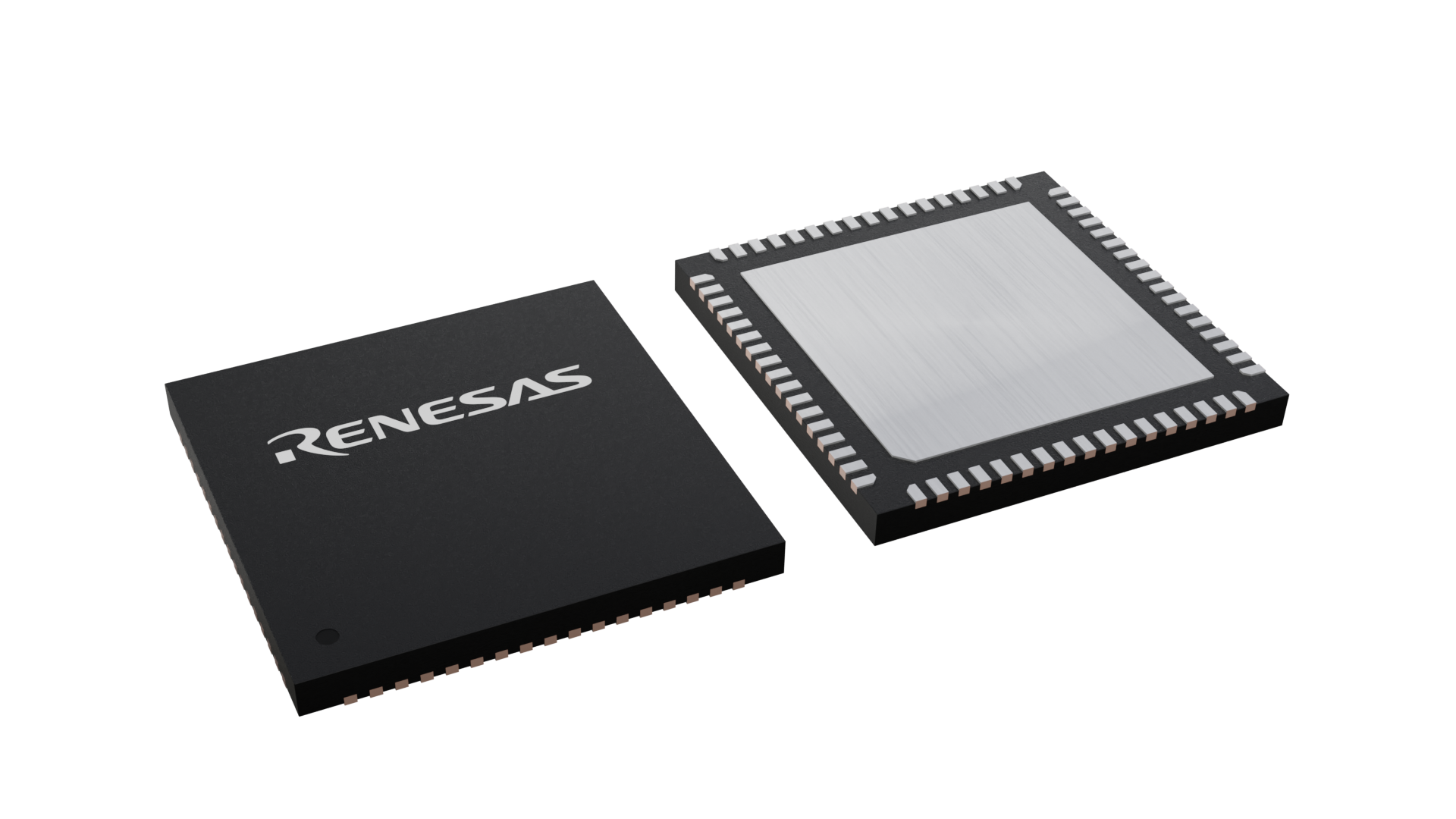

| Pkg. Type: | VFQFPN |
| Pkg. Code: | NLG68 |
| Lead Count (#): | 68 |
| Pkg. Dimensions (mm): | 10.0 x 10.0 x 0.85 |
| Pitch (mm): | 0.5 |
| Pb (Lead) Free | Yes |
| ECCN (US) | EAR99 |
| HTS (US) | 8542.39.0090 |
| Moisture Sensitivity Level (MSL) | 3 |
| Pkg. Type | VFQFPN |
| Lead Count (#) | 68 |
| Pb (Lead) Free | Yes |
| Carrier Type | Tray |
| C-C Jitter Max P-P (ps) | 75 |
| Core Voltage (V) | 2.5 |
| Divider Value | 1, 2, 3, 4, 5, 6, 8, 10, 12 |
| Feedback Divider | 1 - 1, 2 - 2, 4 - 4 |
| Input Freq (MHz) | 4.17 - 250 |
| Input Type | HSTL, LVTTL, LVCMOS, LVPECL |
| Inputs (#) | 2 |
| Length (mm) | 10 |
| MOQ | 84 |
| Moisture Sensitivity Level (MSL) | 3 |
| Output Banks (#) | 5 |
| Output Freq Range (MHz) | 12.5 - 250 |
| Output Signaling | HSTL, LVTTL, LVCMOS |
| Output Skew (ps) | 100 |
| Output Type | HSTL, LVCMOS |
| Output Voltage (V) | 2.5 |
| Outputs (#) | 5 |
| Package Area (mm²) | 100 |
| Pb Free Category | e3 Sn |
| Period Jitter Max P-P (ps) | 75 |
| Pitch (mm) | 0.5 |
| Pkg. Dimensions (mm) | 10.0 x 10.0 x 0.85 |
| Qty. per Carrier (#) | 168 |
| Qty. per Reel (#) | 0 |
| Requires Terms and Conditions | Does not require acceptance of Terms and Conditions |
| Tape & Reel | No |
| Temp. Range (°C) | -40 to 85°C |
| Thickness (mm) | 0.85 |
| VCO Max Freq (MHz) | 250 |
| VCO Min Freq (MHz) | 50 |
| Width (mm) | 10 |
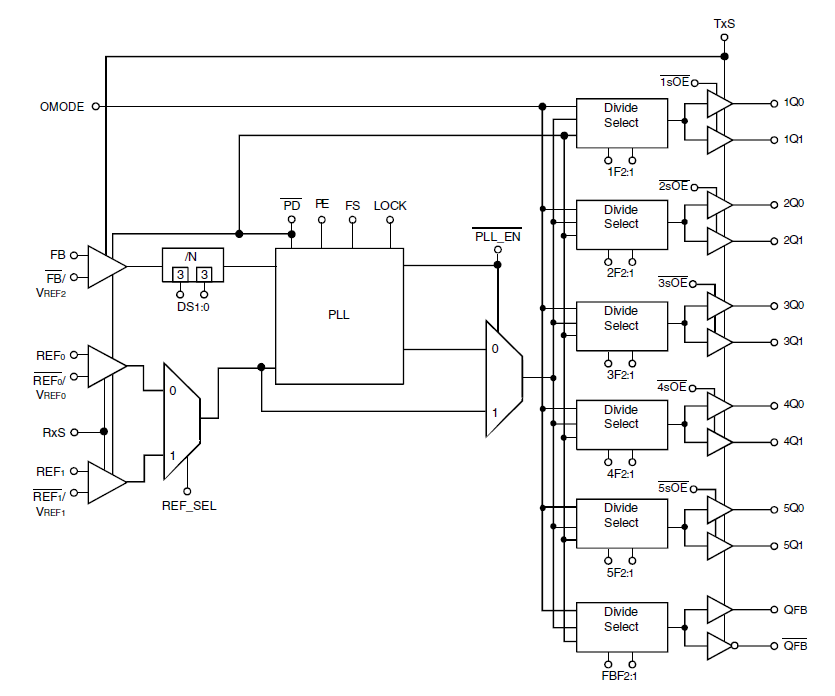
The 5T2010 is a 2.5V PLL clock driver intended for high performance computing and data-communications applications. The 5T2010 has ten outputs in five banks of two, plus a dedicated differential feedback. The redundant input capability allows for a smooth change over to a secondary clock source when the primary clock source is absent. The feedback bank allows divide-by-functionality from 1 to 12 through the use of the DS[1:0] inputs. This provides the user with frequency multiplication 1 to 12 without using divided outputs for feedback. Each output bank also allows for a divide-by functionality of 2 or 4. The 5T2010 features a user-selectable, single-ended or differential input to ten single-ended outputs. The clock driver also acts as a translator from a differential HSTL, eHSTL, 1.8V/2.5V LVTTL, LVEPECL, or single-ended 1.8V/2.5V LVTTL input to HSTL, eHSTL, or 1.8V/2.5V LVTTL outputs. Selectable interface is controlled by 3-level input signals that may be hard-wired to appropriate high-mid-low levels. The outputs can be synchronously enabled/disabled. Furthermore, when PE is held high, all the outputs are synchronized with the positive edge of the REF clock input. When PE is held low, all the outputs are synchronized with the negative edge of REF.