
特性
- 3V to 3.6V operating voltage
- 3.125MHz to 160MHz output frequency range
- Four programmable frequency LVCMOS/LVTTL outputs
- Input from fundamental crystal oscillator or external source
- Balanced drive outputs ±12mA
- PLL disable mode for low frequency testing
- Select inputs (S[1:0]) for divide selection (multiply ratio of 2, 3, 4, 5, 6, 7 and 8)
- 5V tolerant inputs
- Low output skew/jitter
- External PLL feedback, internal loop filter
- -40°C to 85°C ambient operating temperature
- Available in Lead-free (RoHS 6) package
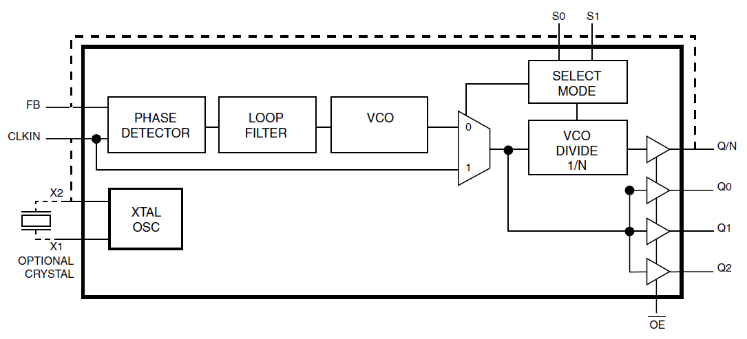
5V925BI - Block Diagram
描述
The 5V925BI is a high-performance, low skew, low jitter phase-locked loop (PLL) clock driver. It provides precise phase and frequency alignment of its clock outputs to an externally applied clock input or internal crystal oscillator. The 5V925BI has been specially designed to interface with Gigabit Ethernet and Fast Ethernet applications by providing a 125MHz clock from 25MHz input. It can also be programmed to provide output frequencies ranging from 3.125MHz to 160MHz with input frequencies ranging from 3.125MHz to 80MHz.


