特性
- High system speed 200MHz (3.1ns clock access time)
- LBO input selects interleaved or linear burst mode
- Self-timed write cycle with global write control (GW), byte write
- enable (BWE), and byte writes (BWx)
- 3.3V core power supply
- Power down controlled by ZZ input
- 3.3V I/O
- Optional - Boundary Scan JTAG Interface (IEEE 1149.1
- compliant)
- Available in 100-pin TQFP, 119-pin BGA and 165 fpBGA packages
描述
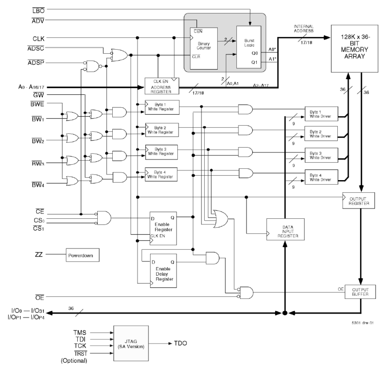
The 71V35761 3.3V CMOS SRAM is organized as 128K x 36. It contains write, data, address and control registers. The burst mode feature offers the highest level of performance to the system designer, as the 71V35761 can provide four cycles of data for a single address presented to the SRAM.
产品参数
| 属性 | 值 |
|---|---|
| Density (Kb) | 4608 |
| Bus Width (bits) | 36 |
| Core Voltage (V) | 3.3 |
| Pkg. Code | BGG119, BQG165, PKG100 |
| Organization | 128K x 36 |
| I/O Voltage (V) | 3.3 - 3.3 |
| I/O Frequency (MHz) | 166 - 166 |
| Temp. Range (°C) | -40 to 85°C, 0 to 70°C |
| Architecture | Synch Burst |
| Output Type | Pipelined |
当前筛选条件

