特性
- High system speed 166MHz (3.5ns clock access time)
- LBO input selects interleaved or linear burst mode
- Self-timed write cycle with global write control (GW), byte
- write enable (BWE), and byte writes (BWx)
- 3.3V core power supply
- Power down controlled by ZZ input
- 2.5V I/O supply (VDDQ)
- Available in 100-pin TQFP and 119-pin BGA packages
描述
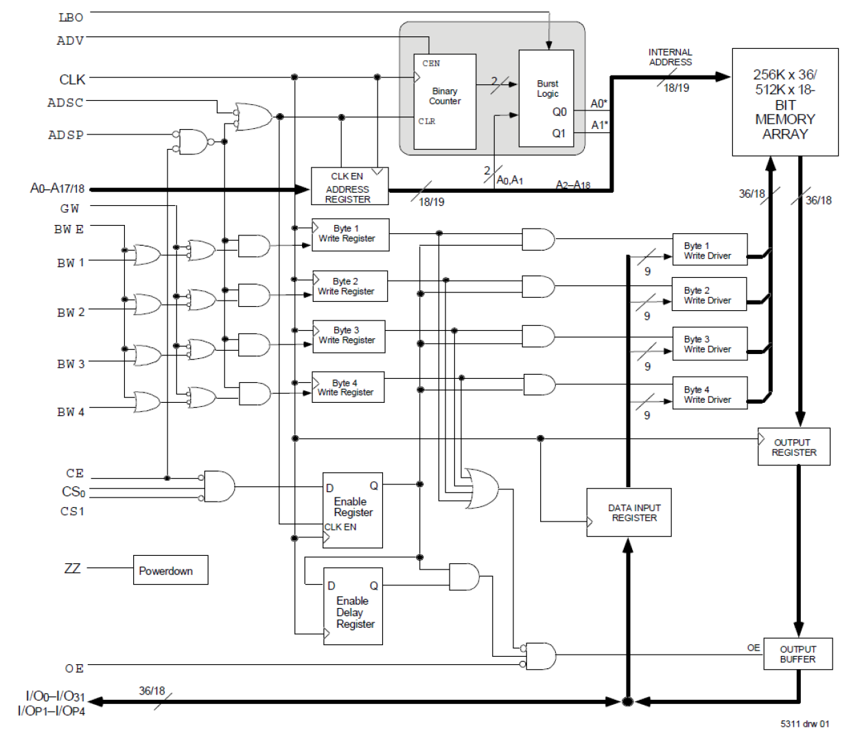
The 71V67602 3.3V CMOS SRAM is organized as 256K x 36. The 71V676 SRAM contains write, data, address and control registers. Internal logic allows the SRAM to generate a self-timed write based upon a decision which can be left until the end of the write cycle. The burst mode feature offers the highest level of performance to the system designer, as it can provide four cycles of data for a single address presented to the SRAM.
产品参数
| 属性 | 值 |
|---|---|
| Density (Kb) | 9216 |
| Bus Width (bits) | 36 |
| Core Voltage (V) | 3.3 |
| Pkg. Code | PKG100 |
| Organization | 256K x 36 |
| I/O Voltage (V) | 3.3 - 3.3 |
| I/O Frequency (MHz) | 150 - 150 |
| Temp. Range (°C) | -40 to 85°C |
| Architecture | Synch Burst |
| Output Type | Pipelined |
封装选项
| Pkg. Type | Pkg. Dimensions (mm) | Lead Count (#) | Pitch (mm) |
|---|---|---|---|
| TQFP | 20.0 x 14.0 x 1.4 | 100 | 0.65 |
当前筛选条件

