特性
- High speed 8:1 differential multiplexer
- One differential LVDS output pair
- Eight selectable differential PCLK, nPCLK input pairs
- PCLKx, nPCLKx pairs can accept the following differential input levels: LVPECL, LVDS, SSTL
- Maximum output frequency: 2.5GHz
- Translates any single ended input signal to LVDS levels with resistor bias on nPCLKx input
- Additive phase jitter, RMS: 0.065ps (typical)
- Part-to-part skew: 300ps (maximum)
- Propagation delay: 600ps (maximum)
- Supply voltage range: 3.135V to 3.465V
- -40°C to 85°C ambient operating temperature
- Available in lead-free (RoHS 6) package
描述
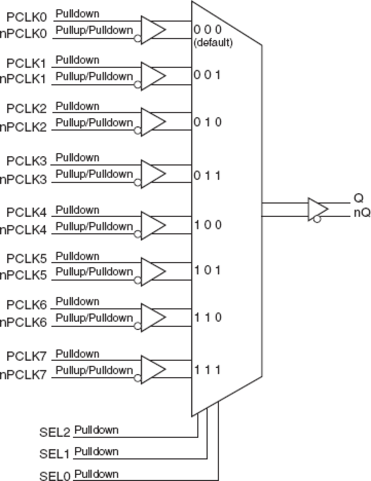
The 854S058I is an 8:1 Differential-to-LVDS Clock Multiplexer which can operate up to 2.5GHz. The 854S058I has 8 selectable differential clock inputs. The PCLK, nPCLK input pairs can accept LVPECL, LVDS or SSTL levels. The fully differential architecture and low propagation delay make it ideal for use in clock distribution circuits. The select pins have internal pulldown resistors. The SEL2 pin is the most significant bit and the binary number applied to the select pins will select the same numbered data input (i.e., 000 selects PCLK0, nPCLK0).
产品参数
| 属性 | 值 |
|---|---|
| Temp. Range (°C) | -40 to 85°C |
| Product Category | Clock Multiplexers |
封装选项
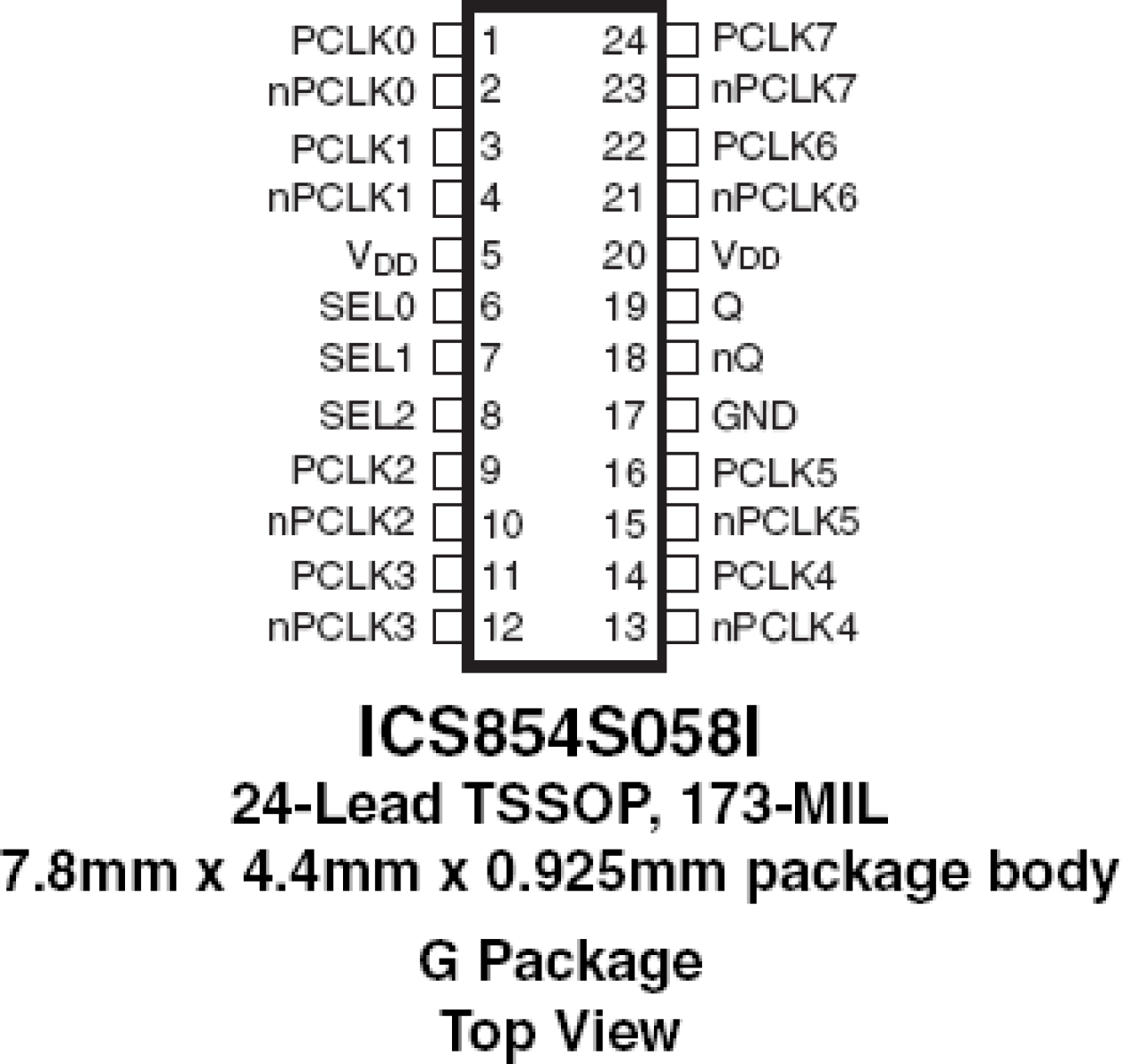
| Pkg. Type | Pkg. Dimensions (mm) | Lead Count (#) | Pitch (mm) |
|---|---|---|---|
| TSSOP | 7.8 x 4.4 x 1.0 | 24 | 0.65 |
当前筛选条件


