
特性
- 5 differential 3.3V LVPECL outputs
- Selectable differential clock inputs
- CLKx, nCLKx pair can accept the following differential input levels: LVPECL, LVDS, LVHSTL, HCSL, SSTL
- Output frequency range: 50MHz to 250MHz
- VCO range: 200MHz to 500MHz
- External feedback for "zero delay" clock regeneration with configurable frequencies
- Cycle-to-cycle jitter (RMS): 20ps (maximum)
- Output skew: 70ps (maximum), within one bank
- 3.3V supply voltage
- -40°C to 85°C ambient operating temperature
- Lead-Free package available
描述
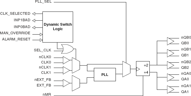
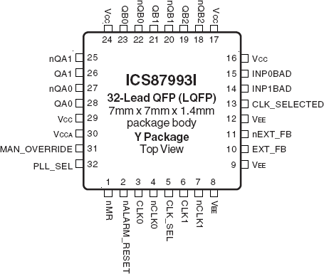
The 87993I is a PLL clock driver designed specifically for redundant clock tree designs. The device receives two differential LVPECL clock signals from which it generates 5 new differential LVPECL clock outputs. Two of the output pairs regenerate the input signal frequency and phase while the other three pairs generate 2x, phase aligned clock outputs. External PLL feedback is used to also provide zero delay buffer performance. The 87993I Dynamic Clock Switch (DCS) circuit continuously monitors both input CLK signals. Upon detection of a failure (CLK stuck HIGH or LOW for at least 1 period), the INP_BAD for that CLK will be latched (H). If that CLK is the primary clock, the DCS will switch to the good secondary clock and phase/frequency alignment will occur with minimal output phase disturbance. The typical phase bump caused by a failed clock is eliminated.


