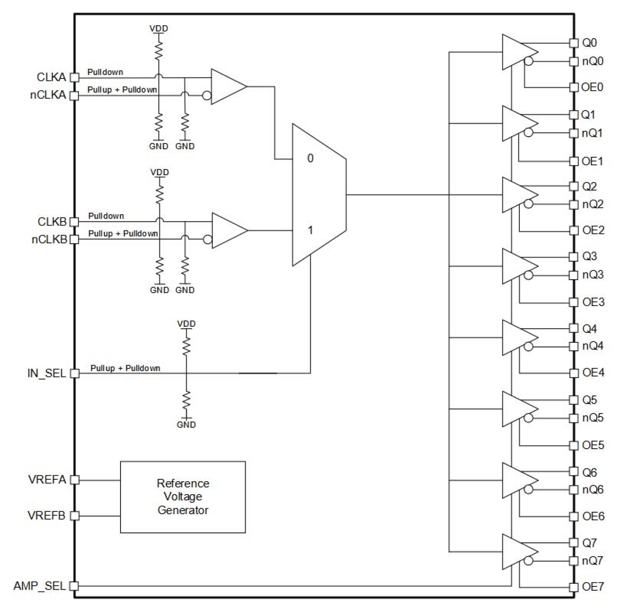
特性
- Eight low skew, low additive jitter LVDS output pairs in two output banks
- Individual OE control pin for each output
- Bank-selectable pin for bank swing output
- Two selectable, differential clock input pairs
- Differential CLK, nCLK pairs can accept LVDS and CML differential input levels
- Maximum input clock frequency of 2GHz
- LVCMOS/LVTTL interface levels for the control input-select pin
- Output skew of 20ps (typical)
- Propagation delay of 450ps (maximum)
- Low propagation delay variation across temperature for 1PPS applications
- Low additive phase jitter, RMS; fREF = 156.25MHz, VPP = 1V, 12kHz to 20MHz: 50fs (typical)
- Device current consumption (IDD): 225mA (typical)
- Full 1.8V or 2.5V supply voltage
- Lead-free (RoHS 6), 40-VFQFPN packaging
- -40 °C to +85 °C ambient operating temperature
- Supports case temperature up to +105 °C
描述
The 8P34S1208-1 is a high-performance differential LVDS fanout buffer. The device is designed for the fanout of 1PPS signals or high-frequency, very low additive phase-noise clock and data signals.
The 8P34S1208-1 supports fail-safe operation and is characterized to operate from a 1.8V or 2.5V power supply. Guaranteed output-to-output and part-to-part skew characteristics make the device ideal for clock distribution applications that demand well-defined performance and repeatability.
Two selectable differential inputs and eight low skew outputs are available. The integrated bias voltage reference enables easy interfacing of single-ended signals to the device inputs. The device is optimized for low power consumption and low additive phase noise.
The 8P34S1208-1 has an individual OE control pin for each output, which provides excellent control over the output enable functions.
产品参数
| 属性 | 值 |
|---|---|
| Temp. Range (°C) | -40 to 85°C |
| Product Category | Clock Buffers & Drivers, RF Buffers |
封装选项
| Pkg. Type | Pkg. Dimensions (mm) | Lead Count (#) | Pitch (mm) |
|---|---|---|---|
| VFQFPN | 6.0 x 6.0 x 0.9 | 40 | 0.5 |
应用
- 4G and 5G radio unit (RU) and distributed unit (DU) systems
- Ethernet switches/routers
- Medical imaging
- Professional audio and video
- Data centers and servers
当前筛选条件

