
特性
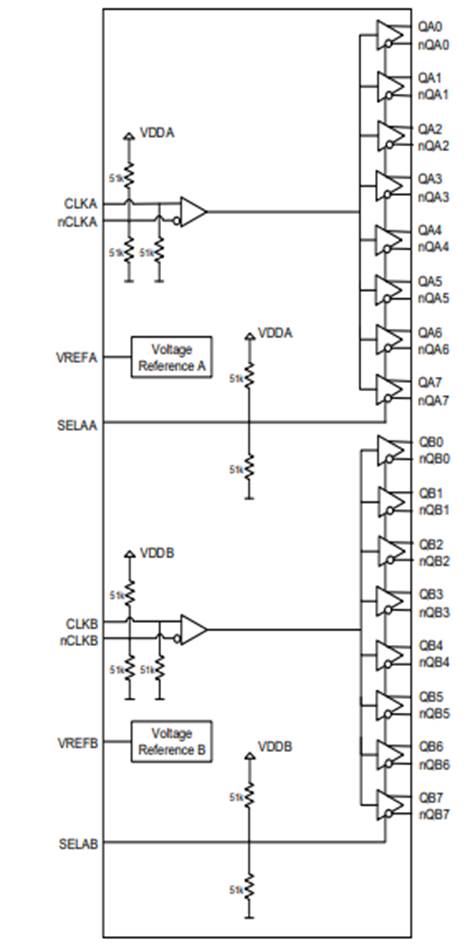
- Dual 1:8 low skew, low additive jitter LVDS fanout buffers
- Matched AC characteristics across both channels
- High isolation between channels
- Low power consumption
- Both differential CLKA, nCLKA and CLKB, nCLKB inputs accept
LVDS, LVPECL and single-ended LVCMOS levels - Maximum input clock frequency: 2GHz
- Output amplitudes: 350mV, 500mV (selectable)
- Output bank skew: 10ps typical
- Output skew: 20ps typical
- Low additive phase jitter, RMS: <45fs typical,
(fREF = 156.25MHz, 12kHz - 20MHz) - Full 1.8V / 2.5V supply voltage mode
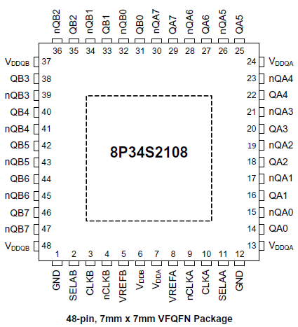
- Lead-free (RoHS 6), 48-lead VFQFN packaging
- -40°C to 85°C (Tc ≤ 105°C) operating temperature range
描述
The 8P34S2108 is a high-performance, low-power, differential dual 1:6 LVDS output 1.8V/2.5V fanout buffer. The device supports fail-safe operation and is designed for the fanout of high-frequency, very low additive phase-noise clock and data signals. Two independent buffer channels are available, each channel has eight low skew outputs. High isolation between channels minimizes noise coupling. AC characteristics such as propagation delay are matched between channels. Guaranteed output-to-output and part-to-part skew characteristics make the 8P34S2108 ideal for those clock distribution applications demanding well-defined performance and repeatability. The device is characterized to operate from a 1.8V/2.5V power supply. The integrated bias voltage references enable easy interfacing of AC-coupled signals to the device inputs.
产品参数
| 属性 | 值 |
|---|---|
| Temp. Range (°C) | -40 to 85°C (Tc ≤ 105°C) |
| Product Category | Clock Buffers & Drivers, RF Buffers |
封装选项
| Pkg. Type | Pkg. Dimensions (mm) | Lead Count (#) | Pitch (mm) |
|---|---|---|---|
| VFQFPN | 7.0 x 7.0 x 0.9 | 48 | 0.5 |