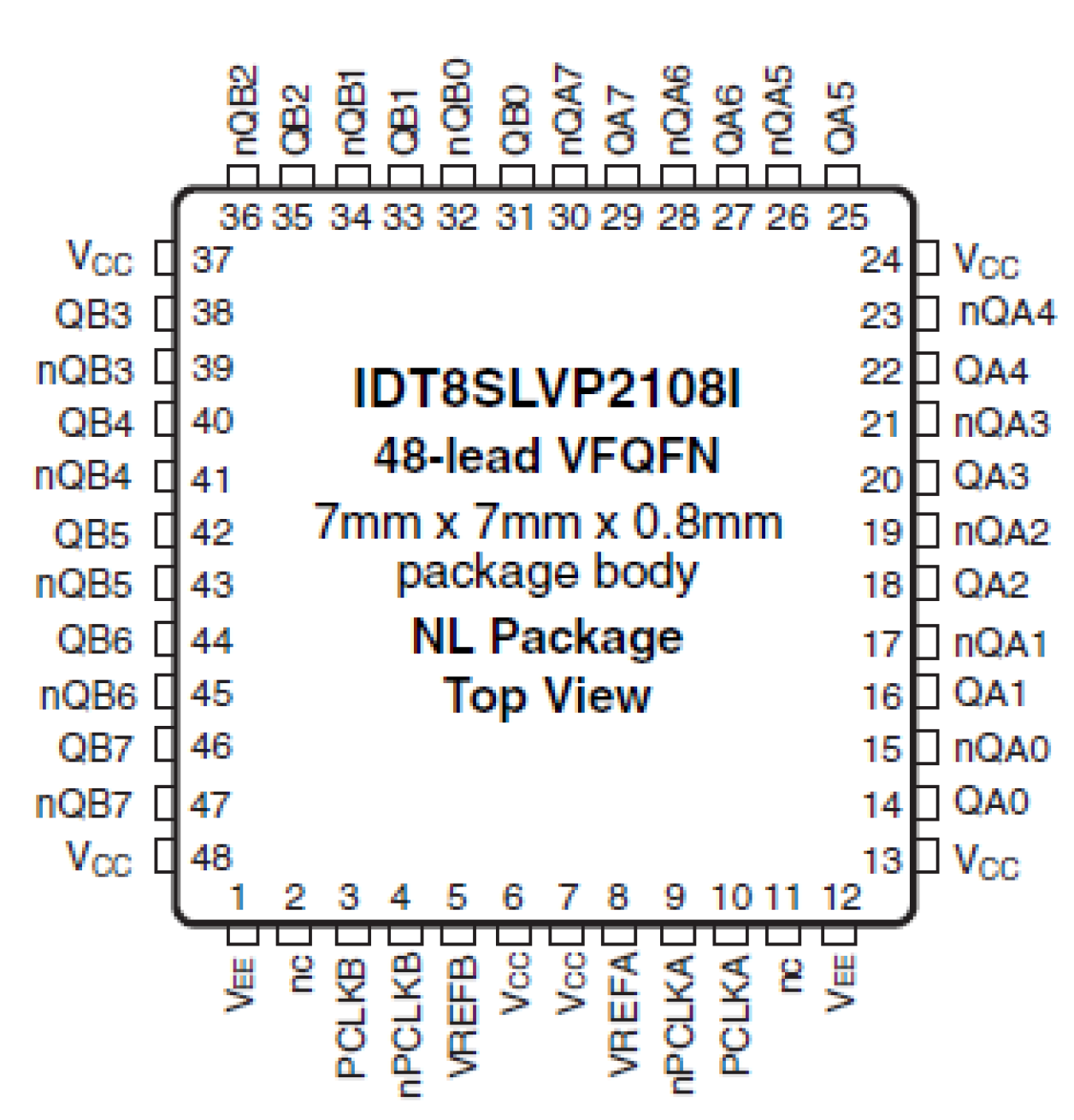
特性
- Two 1:8, low skew, low additive jitter LVPECL fanout buffers
- Two differential clock inputs
- Differential PCLKA, nPCLKA and PCLKB, nPCLKB pairs can accept the following differential input levels: LVDS, LVPECL, CML
- Differential PCLKA, nPCLKA and PCLKB, nPCLKB pairs can also accept single-ended LVCMOS levels.
- Maximum input clock frequency: 2GHz
- Output bank skew: 15ps (typical)
- Propagation delay: 390ps (maximum)
- Low additive phase jitter, RMS: 54fs (maximum) (fREF = 156.25MHz, VPP = 1V, 12kHz to 20MHz, VCC = 3.3V)
- Full 3.3V and 2.5V supply voltage
- Maximum device current consumption (IEE): 143mA
- Available in a Lead-free (RoHS 6), 48-lead VFQFN package
- -40 °C to 85 °C ambient operating temperature
描述
The 8SLVP2108I is a high-performance differential dual 1:8 LVPECL fanout buffer designed for the fanout of high-frequency, very-low additive phase noise clock and data signals. The 8SLVP2108I is characterized for operation from a 3.3V or 2.5V power supply. Guaranteed output-to-output and part-to-part skew characteristics make the 8SLVP2108I ideal for those clock distribution applications demanding well-defined performance and repeatability. Two independent buffers with eight low-skew outputs each are available. The integrated bias voltage references enable easy interfacing of single-ended signals to the device inputs. The device is optimized for low power consumption and low additive phase noise.
产品参数
| 属性 | 值 |
|---|---|
| Temp. Range (°C) | -40 to 85°C |
| Product Category | Clock Buffers & Drivers, RF Buffers |
封装选项
| Pkg. Type | Pkg. Dimensions (mm) | Lead Count (#) | Pitch (mm) |
|---|---|---|---|
| VFQFPN | 7.0 x 7.0 x 0.9 | 48 | 0.5 |
应用方框图
 | 用于 RRU 的 eCPRI 大规模 MIMO eCPRI MIMO RRU 具有低相位噪声、确定性延迟和高定时精度,适用于 5G 网络。 |
当前筛选条件


