封装信息
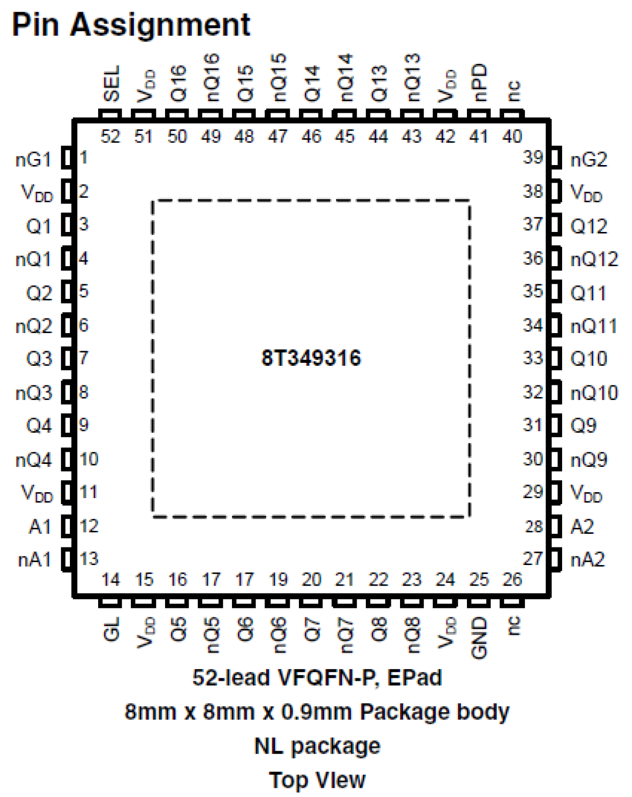
| CAD 模型: | View CAD Model |
| Pkg. Type: | VFQFPN |
| Pkg. Code: | NLG52 |
| Lead Count (#): | 52 |
| Pkg. Dimensions (mm): | 8.0 x 8.0 x 0.9 |
| Pitch (mm): | 0.5 |
环境和出口类别
| Moisture Sensitivity Level (MSL) | 3 |
| Pb (Lead) Free | Yes |
| ECCN (US) | EAR99 |
| HTS (US) | 8542.39.0090 |
产品属性
| Lead Count (#) | 52 |
| Carrier Type | Tray |
| Moisture Sensitivity Level (MSL) | 3 |
| Qty. per Reel (#) | 0 |
| Qty. per Carrier (#) | 260 |
| Pb (Lead) Free | Yes |
| Pb Free Category | e3 Sn |
| Temp. Range (°C) | -40 to 85°C |
| Core Voltage (V) | 2.5 |
| Function | Buffer, Multiplexer |
| Input Freq (MHz) | 1000 - 1000 |
| Input Type | LVTTL, LVPECL, HSTL, HCSL |
| Inputs (#) | 2 |
| Length (mm) | 8 |
| MOQ | 130 |
| Output Banks (#) | 2 |
| Output Freq Range (MHz) | 1000 - 1000 |
| Output Signaling | LVDS |
| Output Skew (ps) | 50 |
| Output Type | LVDS |
| Output Voltage (V) | 2.5 |
| Outputs (#) | 16 |
| Package Area (mm²) | 64 |
| Pitch (mm) | 0.5 |
| Pkg. Dimensions (mm) | 8.0 x 8.0 x 0.9 |
| Pkg. Type | VFQFPN |
| Price (USD) | $14.52346 |
| Product Category | Clock Buffers & Drivers, Clock Multiplexers |
| Requires Terms and Conditions | Does not require acceptance of Terms and Conditions |
| Tape & Reel | No |
| Thickness (mm) | 0.9 |
| Width (mm) | 8 |
有关 8T349316 的资源
描述
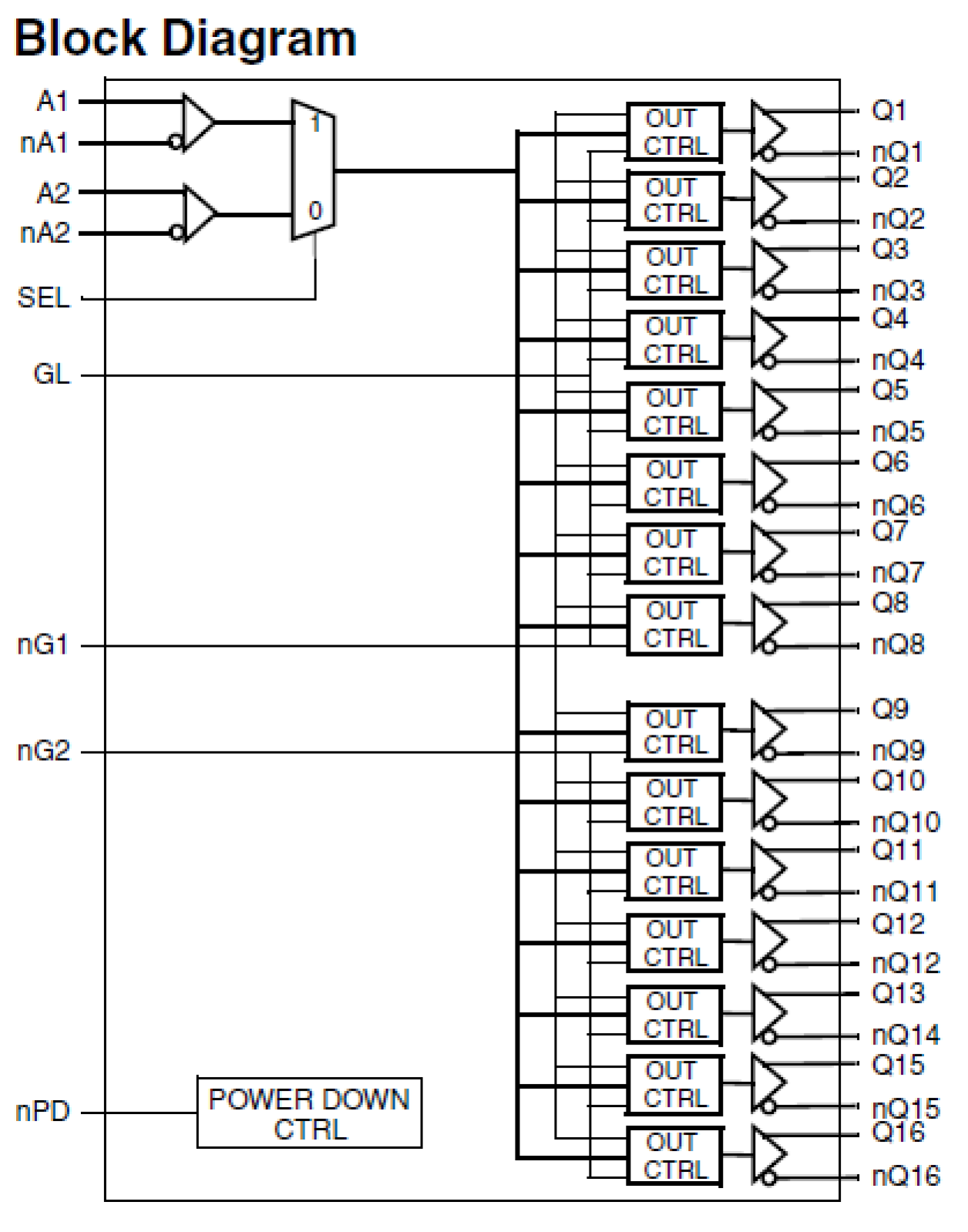
The 8T349316 is a 2.5V differential clock buffer with sixteen LVDS outputs. The fanout from a differential input to the sixteen LVDS outputs reduces loading on the preceding driver and provides an efficient clock distribution network. The 8T349316 can act as a translator from a differential HSTL, LVPECL, CML, or LVDS input to LVDS output signals. A single-ended 3.3V, 2.5V LVCMOS/LVTTL input can also be used to translate to LVDS outputs. The redundant input capability allows for an asynchronous changeover from a primary clock source to a secondary clock source. Selectable reference inputs are controlled by SEL. The 8T349316 outputs can be asynchronously enabled/disabled. When disabled, the outputs will drive to the value selected by the GL pin. Multiple power and grounds reduce noise. The extended temperature range supports wireless infrastructure, telecommunication, and networking end equipment requirements.

