
| CAD 模型: | View CAD Model |
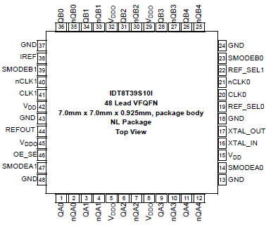
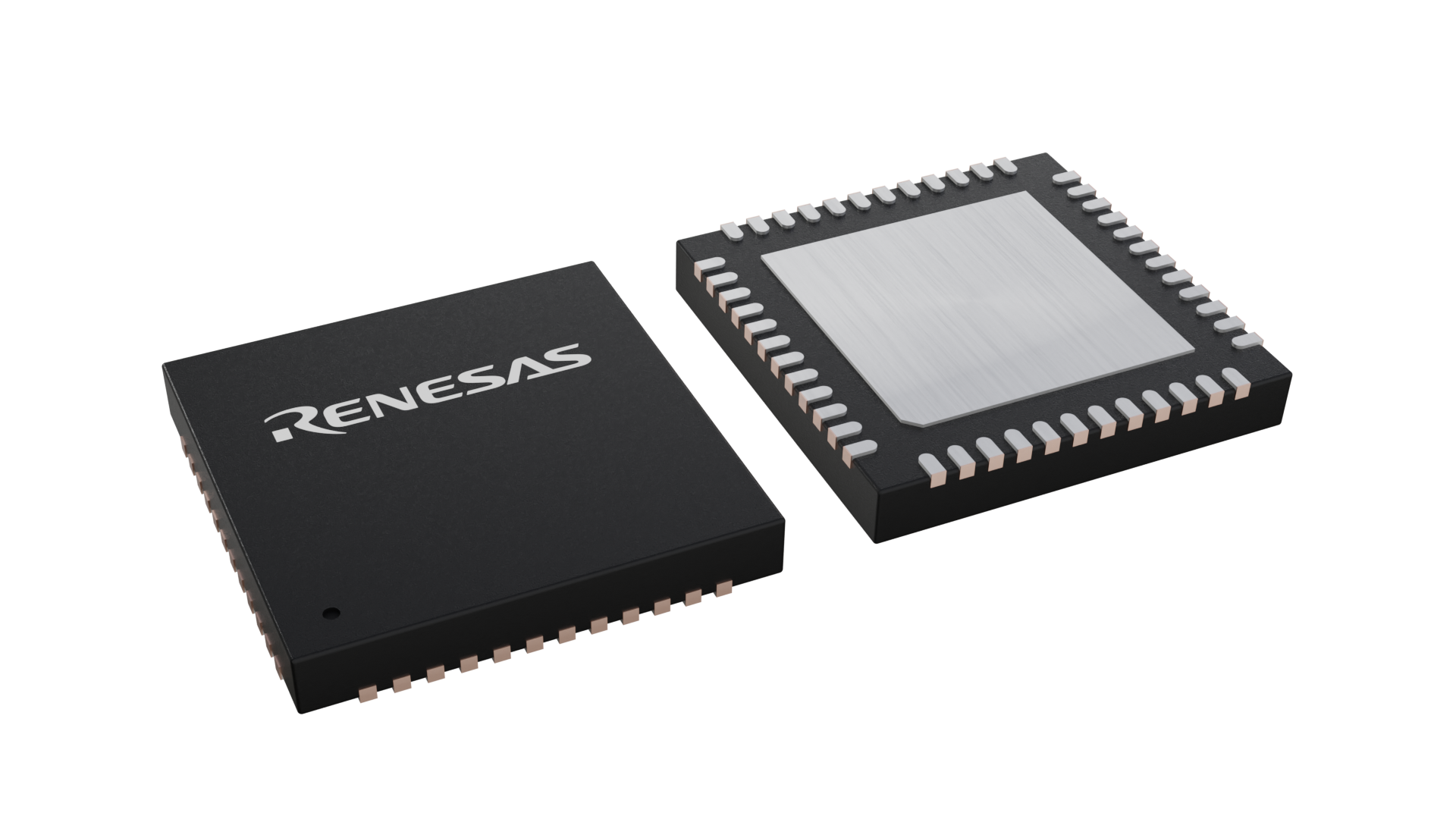
| Pkg. Type: | VFQFPN |
| Pkg. Code: | NLG48 |
| Lead Count (#): | 48 |
| Pkg. Dimensions (mm): | 7.0 x 7.0 x 0.9 |
| Pitch (mm): | 0.5 |
| Moisture Sensitivity Level (MSL) | 3 |
| Pb (Lead) Free | Yes |
| ECCN (US) | EAR99 |
| HTS (US) | 8542.39.0090 |
| Lead Count (#) | 48 |
| Carrier Type | Tray |
| Moisture Sensitivity Level (MSL) | 3 |
| Qty. per Reel (#) | 0 |
| Qty. per Carrier (#) | 260 |
| Pb (Lead) Free | Yes |
| Pb Free Category | e3 Sn |
| Temp. Range (°C) | -40 to 85°C |
| Additive Phase Jitter Typ RMS (fs) | 153 |
| Additive Phase Jitter Typ RMS (ps) | 0.153 |
| Core Voltage (V) | 3.3V, 2.5V |
| Family Name | 8T39S |
| Function | Buffer, Multiplexer |
| Input Freq (MHz) | 2000 |
| Input Type | Crystal, HCSL, LVDS, LVPECL |
| Inputs (#) | 3 |
| Length (mm) | 7 |
| MOQ | 260 |
| Output Banks (#) | 2 |
| Output Freq Range (MHz) | 2000 |
| Output Skew (ps) | 32 |
| Output Type | HCSL, LVCMOS, LVDS, LVPECL |
| Output Voltage (V) | 2.5V, 3.3V |
| Outputs (#) | 11 |
| Package Area (mm²) | 49 |
| Pitch (mm) | 0.5 |
| Pkg. Dimensions (mm) | 7.0 x 7.0 x 0.9 |
| Pkg. Type | VFQFPN |
| Product Category | Clock Buffers & Drivers, Clock Multiplexers |
| Prog. Interface | Pin select |
| Requires Terms and Conditions | Does not require acceptance of Terms and Conditions |
| Tape & Reel | No |
| Thickness (mm) | 0.9 |
| Width (mm) | 7 |
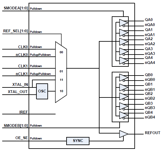
The 8T39S10I is a high-performance clock fanout buffer. The input clock can be selected from two differential inputs or one crystal input. The internal oscillator circuit is automatically disabled if the crystal input is not selected. The crystal pin can be driven by single-ended clock when crystal is bypassed.The selected signal is distributed to ten differential outputs which can be configured as LVPECL, LVDS or HSCL outputs. In addition, an LVCMOS output is provided. All outputs can be disabled into a high-impedance state. The device is designed for signal fanout of high-frequency, low phase-noise clock and data signal. The outputs are at a defined level when inputs are open circuit or tied to ground. It is designed to operate from a 3.3V or 2.5V core power supply, and either a 3.3V or 2.5V output operating supply.