
特性
- Designed for 1PPS, 2kHz, 8kHz, and 10MHz GPS clock signal distribution
- High-speed 1:8 LVDS fanout buffer
- Eight differential LVDS output pairs
- 2:1 input multiplexer
- Two selectable differential inputs accept LVDS and LVPECL signals
- Accepts rectangular and sinusoidal input signals
- Two input monitoring outputs (LVCMOS)
- Max output frequency: 250MHz
- Additive RMS phase jitter: 118fs (typical) at 100MHz (12kHz to 20MHz)
- Part-to-Part skew: 250ps (maximum)
- Propagation delay: 325ps (typical), LVDS output
- Full 2.5V and 3.3V voltage supply
- -40 °C to 85 °C ambient operating temperature
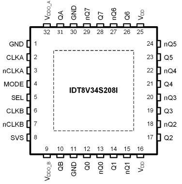
- Lead-free 32-lead VFQFN (RoHS 6/6) packaging
描述
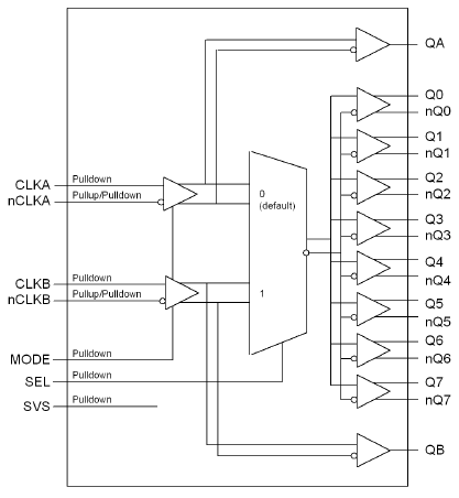
The 8V34S208 is a differential 1:8 LVDS fanout buffer with a 2:1 input multiplexer. The device accepts DC to 250MHz clock and data signals and is designed for 1Hz clock/1PPS, 2kHz, and 8kHz signal distribution. Controlled by the input mode selection pin, the differential input stages accept both rectangular or sinusoidal signals. The 8V34S208 also provides level-translated LVCMOS/LVTTL outputs which are copies of the individual differential inputs CLKA and CLKB. The propagation delay of the device is very low, providing an ideal solution for clock distribution circuits with tight phase alignment requirements. The multiplexer select pin (SEL) allows the selection of one out of two input signals, which is copied to the four differential outputs.