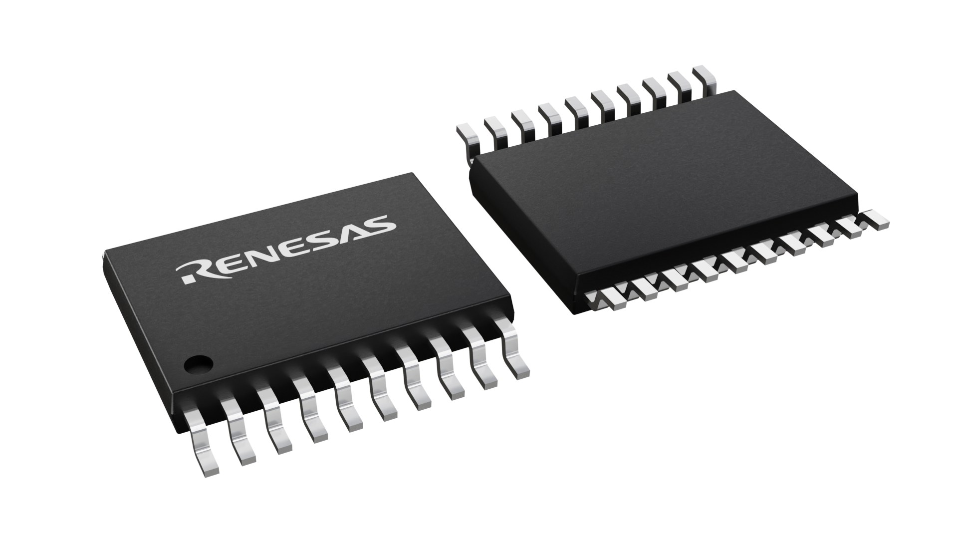

封装信息
| CAD 模型: | View CAD Model |
| Pkg. Type: | TSSOP |
| Pkg. Code: | PGG20 |
| Lead Count (#): | 20 |
| Pkg. Dimensions (mm): | 6.5 x 4.4 x 1.0 |
| Pitch (mm): | 0.65 |
环境和出口类别
| Moisture Sensitivity Level (MSL) | 1 |
| Pb (Lead) Free | Yes |
| ECCN (US) | EAR99 |
| HTS (US) | 8542.39.0090 |
产品属性
| Lead Count (#) | 20 |
| Carrier Type | Tube |
| Moisture Sensitivity Level (MSL) | 1 |
| Qty. per Carrier (#) | 74 |
| Package Area (mm²) | 28.6 |
| Pitch (mm) | 0.65 |
| Pkg. Dimensions (mm) | 6.5 x 4.4 x 1.0 |
| Qty. per Reel (#) | 0 |
| Pb (Lead) Free | Yes |
| Pb Free Category | e3 Sn |
| Temp. Range (°C) | 0 to 70°C |
| Assembly Location | TAIWAN |
| Wafer Fab Location | SINGAPORE |
| Accepts Spread Spec Input | Yes |
| Advanced Features | HW PLL mode control |
| App Jitter Compliance | PCIe Gen1, PCIe Gen2, PCIe Gen3 |
| Architecture | Common |
| C-C Jitter Max P-P (ps) | 50 |
| C-C Jitter Typ P-P (ps) | 25 |
| Chipset Name | Blackford, Clarksboro, Greencreek, Lindenhurst, Twincastle, San Clemente, Seaburg, Tylersburg |
| Core Voltage (V) | 3.3 |
| Diff. Input Signaling | HCSL |
| Diff. Inputs | 1 |
| Diff. Output Signaling | HCSL |
| Diff. Outputs | 2 |
| Diff. Termination Resistors | 8 |
| Feedback Input | No |
| Function | Zero Delay Buffer |
| Input Freq (MHz) | 50 - 100 |
| Input Type | HCSL |
| Inputs (#) | 1 |
| Length (mm) | 6.5 |
| MOQ | 222 |
| Multiplication Value | 1 |
| Output Banks (#) | 1 |
| Output Freq Range (MHz) | 10 - 110 |
| Output Skew (ps) | 25 |
| Output Type | HCSL |
| Output Voltage (V) | 0.8 |
| Outputs (#) | 2 |
| PLL | Yes |
| Pkg. Type | TSSOP |
| Platform Name | Bensley, Caneland, Glidewell, Lindenhurst, Truland, Stoakley, Thurley, Cranberry Lake |
| Power Consumption Typ (mW) | 231 |
| Price (USD) | $4.54 |
| Product Category | PCI Express Clocks |
| Prog. Clock | No |
| Requires Terms and Conditions | Does not require acceptance of Terms and Conditions |
| Supply Voltage (V) | 3.3 - 3.3 |
| Tape & Reel | No |
| Thickness (mm) | 1 |
| Width (mm) | 4.4 |
有关 9DB233 的资源
描述
The 9DB233 zero delay buffer (ZDB) supports PCIe Gen3 requirements while being backward compatible with PCIe Gen2 and Gen1. The 9DB233 is driven by a differential SRC output pair from a 932S421 or 932SQ420 or equivalent main clock generator. It attenuates jitter on the input clock and has a selectable PLL bandwidth to maximize performance in systems with or without spread spectrum clocking. An SMBus interface allows control of the PLL bandwidth and bypass options, while two clock request (OE#) pins make the 9DB233 suitable for Express Card applications.