特性
- Single 1.7V - 2.0V Supply
- 128Mbit (16 x 8 Mbit physical block) Flash Memory
- Serial Peripheral Interface (SPI) and Quad Peripheral Interface (QPI) Compatible
- Supports SPI Modes 0 and 3
- Supports Dual Output Read and Quad I/O Program and Read
- Supports QPI Program and Read
- 133MHz Maximum Operating Frequency
- Clock-to-Output (tV1 ) of 6ns
- Up to 65Mbytes/s Continuous Data Transfer Rate
- Quad Enabled
- Full Chip Erase
- Flexible, Optimized Erase Architecture for Code and Data Storage Applications
- 0.6ms Typical Page Program (256 bytes) Time
- 60ms Typical 4kB Block Erase Time
- 200ms Typical 32kB Block Erase Time
- 350ms Typical 64kB Block Erase Time
- Hardware Controlled Locking of Status Registers via WP Pin
- 4kbit Secured One-Time Programmable Security Register
- Hardware Write Protection
- Serial Flash Discoverable Parameters (SFDP) Register
- Flexible Programming
- Byte/Page Program (1 to 256 bytes)
- Dual or Quad Input Byte/Page Program (1 to 256 bytes)
- Erase/Program Suspend and Resume
- JEDEC Standard Manufacturer and Device ID Read Methodology
- Low Power Dissipation
- 2μA Deep Power-Down Current (Typical)
- 10μA Standby Current (Typical)
- 5mA Active Read Current (Typical)
- Endurance: 100,000 program/erase cycles (4kbyte, 32kbyte, or 64kbyte blocks)
- Data Retention: 20 Years
- Industrial Temperature Range: -40°C to +85°C
- Industry Standard Green (Pb/Halide-free/RoHS-Compliant) Package Options
- 8-Pad DFN (6mm x 5mm x 0.6mm)
- 8-Lead SOIC (208mil)
- 21-Ball WLCSP
- 21-Ball Low-Profile WLCSP

描述
The AT25QL128A is a member of our standard class code and data storage solutions designed for low-voltage systems in which program code is shadowed from Flash memory into embedded or external RAM for execution.
The architecture includes standard erase block sizes and a security register for unique device serialization, system-level Electronic Serial Number (ESN) storage, locked key storage, etc.
The AT25QL128A is Quad enabled at the factory and offers a universally compatible pinout and command set, standard block architecture, and continuous read, wrap, and burst modes for XiP.
Renesas Boards & Kits
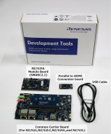
RZ/G2UL MPU 评估板套件
该评估板套件适用于评估 RZ/G2UL。 RZ/G2UL 评测板套件由模块板(SOM)和扩展板组成。 模块板符合 SMARC v2.1 标准。
配件:
- RZ/G2UL 模块板(SMARC2.1)
- 公共载板(用于 RZ/G2L、RZ/G2LC、RZ/G2UL 和 RZ/V2L)
- USB 数据线(USB Type-A、Micro USB Type-B)
*请自行准备以下设备:
- 65W USB Type-C 充电器
- USB PD 接口
- 输出:5V3A,9V3A,15V3A,20V3.25A
- USB Type-C 转 Type-C 电缆
- USB-C 和 USB-C 3.1 Gen2 USB-PD 100W... 阅读详情
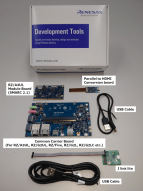
RZ/A3UL 评估板套件
此评估板套件特别适用于评估 RZ/A3UL。 RZ/A3UL 评估板套件由模块板 (SOM) 和扩展板组成。 SOM 符合 SMARC v2.1 标准。
有两种类型的评估板:QSPI版本和Octal SPI版本。
- QSPI版本:内存配置/QSPI串行闪存(Boot) + DDR4:RTK9763U02S01002BE
- Octal-SPI版本:内存配置/ Octa 闪存(Boot) + Octa RAM + DDR4:RTK9763U02S01003BE
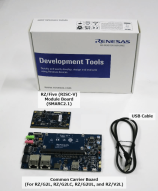
RZ/Five 评估板套件
筛选
Partner Solutions
 Development Tool中文µISP is a compact standalone and universal solution, specifically designed for production environments, based on Algocrafts WriteNow! Technology. This is a standard tool for many families and devices and supports multi programming protocol (JTAG, SPI, UART, DAP, SWD, I2C, BDM, custom protocol, etc).提供方: Algocraft Srl
- Development Tool中文WriteNow! Series of In-System Programmers is a breakthrough in the programming industry. The programmers support a large number of devices (microcontrollers, memories, CPLDs and other programmable devices) from various manufacturers and have a compact size for easy ATE/fixture integration. They work in standalone or connected to a ...提供方: Algocraft Srl
No Results Found.
确保所有关键词拼写正确。
尝试使用更少、不同或更宽泛的词语来改变搜索结果。
如果您使用了筛选器,请考虑取消选择某些筛选器选项以扩大搜索结果。
- 搜索我们丰富的知识库,帮助您解答常见问题
- 前往支持论坛,获取瑞萨电子技术专家和社群的帮助
No Results Found.
确保所有关键词拼写正确。
尝试使用更少、不同或更宽泛的词语来改变搜索结果。
如果您使用了筛选器,请考虑取消选择某些筛选器选项以扩大搜索结果。
- 搜索我们丰富的知识库,帮助您解答常见问题
- 前往支持论坛,获取瑞萨电子技术专家和社群的帮助
No Results Found.
确保所有关键词拼写正确。
尝试使用更少、不同或更宽泛的词语来改变搜索结果。
如果您使用了筛选器,请考虑取消选择某些筛选器选项以扩大搜索结果。
- 搜索我们丰富的知识库,帮助您解答常见问题
- 前往支持论坛,获取瑞萨电子技术专家和社群的帮助
No Results Found.
确保所有关键词拼写正确。
尝试使用更少、不同或更宽泛的词语来改变搜索结果。
如果您使用了筛选器,请考虑取消选择某些筛选器选项以扩大搜索结果。
- 搜索我们丰富的知识库,帮助您解答常见问题
- 前往支持论坛,获取瑞萨电子技术专家和社群的帮助
- Development Tool中文µISP is a compact standalone and universal solution, specifically designed for production environments, based on Algocrafts WriteNow! Technology. This is a standard tool for many families and devices and supports multi programming protocol (JTAG, SPI, UART, DAP, SWD, I2C, BDM, custom protocol, etc).提供方: Algocraft Srl
- Development Tool中文WriteNow! Series of In-System Programmers is a breakthrough in the programming industry. The programmers support a large number of devices (microcontrollers, memories, CPLDs and other programmable devices) from various manufacturers and have a compact size for easy ATE/fixture integration. They work in standalone or connected to a ...提供方: Algocraft Srl
