特性
- Wide operating voltage range of 4.5V to 13.2V
- Up to 14.7V logic inputs (regardless of VDD level)
- Inverting and non-inverting inputs
- Optimized to drive enhancement mode GaN FETs
- Internal 4.5V regulated gate drive voltage
- Independent outputs for adjustable turn-on/turn-off speeds
- Full military temperature range operation
- TA = -55°C to +125°C
- TJ = -55°C to +150°C
- Radiation hardness assurance (wafer-by-wafer)
- High Dose Rate (HDR) (50-300rad(Si)/s): 100krad(Si) (ISL70040SEH only)
- Low Dose Rate (LDR) (0.01rad(Si)/s): 75krad(Si)
- SEE hardness (refer to the ISL70040SEH, ISL73040SEH SEE Test Report for details)
- No SEB/L LETTH, VDD = 14.7V: 86MeV•cm2/mg
- No SET, LETTH, VDD = 13.2V: 86MeV•cm2/mg
- Electrically screened to DLA SMD 5962-17233

描述
The ISL73040SEH is a low-side driver designed to drive enhancement mode Gallium Nitride (GaN) FETs in isolated topologies and boost-type configurations. The device has a 4.5V gate drive voltage (VDRV) generated using an internal regulator, which prevents the gate voltage from exceeding the maximum gate-source rating of enhancement mode GaN FETs. The gate drive voltage also features an undervoltage lockout (UVLO) protection that ignores the inputs (IN/INB) and keeps OUTL turned on to ensure the GaN FET is in an OFF state whenever VDRV is below the UVLO threshold. The ISL73040SEH's input can withstand voltages up to 14.7V regardless of the VDD voltage, allowing it to be connected directly to most PWM controllers. The ISL73040SEH's split outputs offer the flexibility to adjust the turn-on and turn-off speed independently by adding additional impedance to the turn-on/off paths. The device operates across the military temperature range from -55°C to +125°C and is offered in an 8 Ld hermetically sealed ceramic Surface Mount Device (SMD) package or die form.
产品参数
| 属性 | 值 |
|---|---|
| Rating | Space |
| Driver Type | Low Side |
| FET Type | GaNFET |
| Input VCC (Min) (V) | 4.5 |
| Input VCC (Max) (V) | 13.2 |
| Low Side Rise Time (max) (ns) | 90 |
| Low Side Fall Time (max) (ns) | 50 |
| Drivers (#) | 1 |
| Output Type | Inverting/Non-inverting |
| Peak Output Source Current (A) | 1.5 |
| Peak Output Sink Current (A) | 2.8 |
| Gate Drive (V) | 4.5 |
| Temp. Range (°C) | -40 to +105°C, -55 to +125°C |
| TID LDR (krad(Si)) | 75 |
| DSEE (MeV·cm2/mg) | 86 |
| Flow | RH Hermetic |
| Qualification Level | Class V, EM |
| Die Sale Availability? | Yes |
| PROTO Availability? | Yes |
应用
- Flyback and forward converters
- Boost and PFC converters
- Secondary synchronous FET drivers
Renesas Boards & Kits
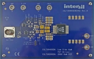
Radiation Hardened ISL73040SEH GaN FET Driver & ISL73024SEH GaN Power Transistor Evaluation Platform (200V GaN FET)
The ISL73040SEHEV4Z evaluation board demonstrates how to build a half-bridge power stage with the ISL73040SEH low-side GaN driver and the ISL73024SEH 200V GaN FET. The ISL73040SEH has a 4.5V gate drive voltage (VDRV) generated using an internal regulator that prevents the gate voltage from... 阅读详情
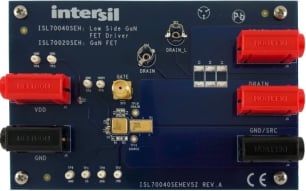
Radiation Hardened ISL70040SEH GaN FET Driver & ISL70020SEH GaN Power Transistor Evaluation Platform (40V GaN FET)
The ISL70040SEHEV5Z evaluation platform is designed to evaluate the ISL70040SEH GaN FET driver alongside the ISL70020SEH GaN power transistor. The ISL70040SEH is designed to drive enhancement-mode Gallium Nitride (GaN) FETs in isolated topologies and boost-type configurations. The board operates... 阅读详情
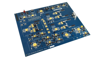
Power Management Reference Design for AMD Versal XQRVC1902
The ISLVERSALDEMO2Z board provides power management for the AMD Xilinx Space Grade Versal ACAP AI Core VC1902 using Renesas' radiation hardened power management devices. The Versal ACAP system requires various supply rails, including the core, digital, analog, and DDR memory. The ISLVERSALDEMO2Z... 阅读详情


