特性
- DDR5 MRDIMM server speeds up to 12800MT/s
- Supports 1 or 2 ranks per pseudo-channel in both x4 and x8 mux mode
- Supports up to 4 ranks in Rank Mode
- Supports SDP, DDP, and 3DS DRAM types
- Provides access to internal control words for configuring device features and adapting to different system applications
- Link CRC protection and descrambling of DCA bus
- DFE/CTLE self-training mode
- I2C/I3C sideband access for asynchronous register access control
- BCOM data buffer control
- Loopback and pass-through modes
- Package: 8.7 × 14.4mm, 264-FCBGA
描述
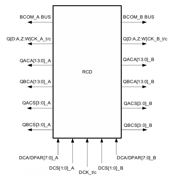
The RRG5012X-A00 is a second-generation Multiplexing Registering Clock Driver (MRCD) used on DDR5 MRDIMMs. Its primary function is to buffer the Command/Address (CA) bus, chip selects, and clock between the host controller and the DRAMs. It also creates a BCOM bus that controls the data buffers. The RRG5012X-A00 contains two separate channels with some common logic such as clocking, but which otherwise operate independently of each other. For each channel, the host interface is a 7-bit + parity/CRC CA bus with two chip-select inputs, running at single or double data rate and 1x or 2x the DRAM frequency.
Both Mux Mode and Rank Mode are supported. In Mux Mode, up to two ranks per each of two multiplexed pseudo-channels are supported, allowing simultaneous operation in the same direction. The RRG5012X-A00 demultiplexes the pseudo-channels and transmits each to a separate DRAM output interface. Rank Mode does not use pseudo-channels and operates as a four-rank LRDIMM.
Each DRAM interface is a 14-bit single data rate CA bus output with a chip-select. The RRG5012X-A00 also transcodes commands from the CA bus onto a per-channel BCOM bus for data buffer control. The RRG5012X-A00 has a common clock input and PLL, but produces eight separate clock pairs to the DRAM channels.
产品参数
| 属性 | 值 |
|---|---|
| Product Type | Registering Clock Driver |
| Function | DDR5 Gen 2 MRDIMM MRCD |
| Application System | Server |
封装选项
| Pkg. Type | Pkg. Dimensions (mm) | Lead Count (#) | Pitch (mm) |
|---|---|---|---|
| FCCSP | 8.7 x 14.4 x 0.9 | 264 | 0.6 |
应用
- MRDIMM Modules for Enterprise Servers
- 数据手册 - 精简版英语RRG5012X-A00 Short-Form DatasheetRECOMMENDEDPDF 108 KB R10DO0015EU0100 Rev.1.00 2024年4月19日The RRG5012X-A00 MRCD is a second-generation Multiplexing Registering Clock Driver used on DDR5 MRDIMMs that enables high-speed DDR5 MRDIMM operation by buffering command, address, chip-select, and clock signals between the host and DRAM. It supports dual independent channels, flexible mux and rank modes, and up to 12800MT/s speeds. The device optimizes signal integrity, controls data buffers via BCOM, and adapts to advanced server memory configurations.
推荐文档 (1)
- 数据手册 - 精简版英语RRG5012X-A00 Short-Form DatasheetRECOMMENDEDPDF 108 KB R10DO0015EU0100 Rev.1.00 2024年4月19日The RRG5012X-A00 MRCD is a second-generation Multiplexing Registering Clock Driver used on DDR5 MRDIMMs that enables high-speed DDR5 MRDIMM operation by buffering command, address, chip-select, and clock signals between the host and DRAM. It supports dual independent channels, flexible mux and rank modes, and up to 12800MT/s speeds. The device optimizes signal integrity, controls data buffers via BCOM, and adapts to advanced server memory configurations.
数据手册 (1)
No Results Found.
确保所有关键词拼写正确。
尝试使用更少、不同或更宽泛的词语来改变搜索结果。
如果您使用了筛选器,请考虑取消选择某些筛选器选项以扩大搜索结果。
- 搜索我们丰富的知识库,帮助您解答常见问题
- 前往支持论坛,获取瑞萨电子技术专家和社群的帮助
No Results Found.
确保所有关键词拼写正确。
尝试使用更少、不同或更宽泛的词语来改变搜索结果。
如果您使用了筛选器,请考虑取消选择某些筛选器选项以扩大搜索结果。
- 搜索我们丰富的知识库,帮助您解答常见问题
- 前往支持论坛,获取瑞萨电子技术专家和社群的帮助
No Results Found.
确保所有关键词拼写正确。
尝试使用更少、不同或更宽泛的词语来改变搜索结果。
如果您使用了筛选器,请考虑取消选择某些筛选器选项以扩大搜索结果。
- 搜索我们丰富的知识库,帮助您解答常见问题
- 前往支持论坛,获取瑞萨电子技术专家和社群的帮助
No Results Found.
确保所有关键词拼写正确。
尝试使用更少、不同或更宽泛的词语来改变搜索结果。
如果您使用了筛选器,请考虑取消选择某些筛选器选项以扩大搜索结果。
- 搜索我们丰富的知识库,帮助您解答常见问题
- 前往支持论坛,获取瑞萨电子技术专家和社群的帮助
No Results Found.
确保所有关键词拼写正确。
尝试使用更少、不同或更宽泛的词语来改变搜索结果。
如果您使用了筛选器,请考虑取消选择某些筛选器选项以扩大搜索结果。
- 搜索我们丰富的知识库,帮助您解答常见问题
- 前往支持论坛,获取瑞萨电子技术专家和社群的帮助
No Results Found.
确保所有关键词拼写正确。
尝试使用更少、不同或更宽泛的词语来改变搜索结果。
如果您使用了筛选器,请考虑取消选择某些筛选器选项以扩大搜索结果。
- 搜索我们丰富的知识库,帮助您解答常见问题
- 前往支持论坛,获取瑞萨电子技术专家和社群的帮助
No Results Found.
确保所有关键词拼写正确。
尝试使用更少、不同或更宽泛的词语来改变搜索结果。
如果您使用了筛选器,请考虑取消选择某些筛选器选项以扩大搜索结果。
- 搜索我们丰富的知识库,帮助您解答常见问题
- 前往支持论坛,获取瑞萨电子技术专家和社群的帮助
No Results Found.
确保所有关键词拼写正确。
尝试使用更少、不同或更宽泛的词语来改变搜索结果。
如果您使用了筛选器,请考虑取消选择某些筛选器选项以扩大搜索结果。
- 搜索我们丰富的知识库,帮助您解答常见问题
- 前往支持论坛,获取瑞萨电子技术专家和社群的帮助
No Results Found.
确保所有关键词拼写正确。
尝试使用更少、不同或更宽泛的词语来改变搜索结果。
如果您使用了筛选器,请考虑取消选择某些筛选器选项以扩大搜索结果。
- 搜索我们丰富的知识库,帮助您解答常见问题
- 前往支持论坛,获取瑞萨电子技术专家和社群的帮助
No Results Found.
确保所有关键词拼写正确。
尝试使用更少、不同或更宽泛的词语来改变搜索结果。
如果您使用了筛选器,请考虑取消选择某些筛选器选项以扩大搜索结果。
- 搜索我们丰富的知识库,帮助您解答常见问题
- 前往支持论坛,获取瑞萨电子技术专家和社群的帮助
No Results Found.
确保所有关键词拼写正确。
尝试使用更少、不同或更宽泛的词语来改变搜索结果。
如果您使用了筛选器,请考虑取消选择某些筛选器选项以扩大搜索结果。
- 搜索我们丰富的知识库,帮助您解答常见问题
- 前往支持论坛,获取瑞萨电子技术专家和社群的帮助
No Results Found.
确保所有关键词拼写正确。
尝试使用更少、不同或更宽泛的词语来改变搜索结果。
如果您使用了筛选器,请考虑取消选择某些筛选器选项以扩大搜索结果。
- 搜索我们丰富的知识库,帮助您解答常见问题
- 前往支持论坛,获取瑞萨电子技术专家和社群的帮助