
特性
- 第四代技术
- 符合 JEDEC 标准的 GaN 技术
- Dynamic RDS(on)eff 经过生产测试
- 坚固的设计,定义
- 宽栅极安全裕度
- 瞬态过压能力
- 非常低的 QRR
- 减少分频损耗
- 在硬开关和软开关电路中实现更高的效率
- 提高功率密度
- 减小系统尺寸和重量
- 总体降低系统成本
- 使用常用栅极驱动器易于驱动
- GSD 引脚布局改善了高速设计
- 符合 RoHS 标准和无卤素包装
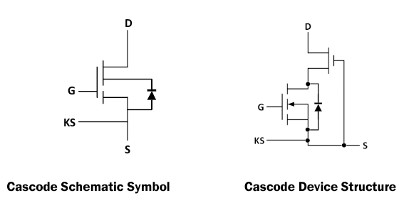
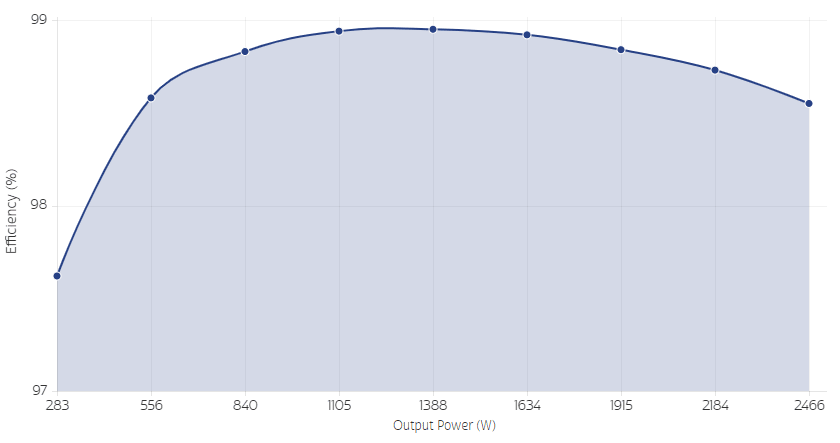
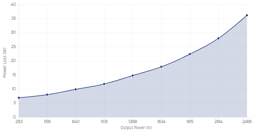
TP65H070G4LSGB Typical Diagram
描述
TP65H070G4LSGB 650V 72mΩ 氮化镓 (GaN) FET 是使用我们的 Gen IV 平台构建的常闭器件。 它结合了最先进的高压 GaN HEMT 和低压硅 MOSFET 技术,提供卓越的可靠性和性能。
瑞萨电子的 GaN 功率产品通过更低的栅极电荷、更低的交越损耗和更小的反向恢复电荷,提供比硅更高的效率。
TP65H070G4LSGB采用行业标准的 PQFN88 封装,具有通用的源封装配置。
应用
- 数据通信
- 博大实业
- 光伏逆变器
- 伺服电机
- 消费领域
- 计算
| 器件号 | 状态 | 样品 | 库存 | 封装 | Carrier Type | Moisture Sensitivity Level (MSL) | Mounting Type | Temp. Range (°C) |
|---|---|---|---|---|---|---|---|---|
| TP65H070G4LSGB | NRND | N/A | 缺货 | PQFN88 | Tape & Reel | 3 | Surface Mount | -55 to +150°C |
加载中
- 白皮书英语PDF 1.9 MB R16WP0012EU0100 Rev.1.00 2025年12月19日D-Mode GaN combines the best of both GaN and Silicon and is ideal for high-voltage applications with high-speed, high-voltage GaN switching, robust 4V threshold gate compatible with standard gate drivers, and a range of standard package offerings not available with other GaN technologies.
- 技术摘要英语PDF 992 KB R16TB0004EU0100 Rev.1.00 2025年12月02日
- 数据手册英语TP65H070G4LSGBEA DatasheetRECOMMENDEDPDF 818 KB R07DS1619EU0200 Rev.2.00 2025年11月25日The TP65H070G4LSGBEA 650V, 72mΩ Gallium Nitride (GaN) FET is a normally-off device combining a high-voltage D-mode GaN HEMT and low-voltage silicon MOSFET. It offers enhanced noise immunity with a 4V threshold voltage with no negative gate drive required. The Renesas Gen IV SuperGaN® platform uses advanced epi to improve efficiency over silicon via lower gate charge, output capacitance, crossover loss, and reverse recovery charge.
- 应用说明英语PDF 372 KB 2024年12月11日AI 生成的摘要: GaN power switches require careful PCB layout and probing techniques to fully utilize their fast switching capabilities. Minimizing parasitic inductances and capacitances in the power and gate drive loops reduces ringing and ensures stable operation. A large ground plane, close placement of power components, and short, wide traces in the gate drive circuit improve performance. Accurate probing demands short ground leads and direct probe placement to avoid measurement artifacts. Avoid adding parasitics during probing by using floating oscilloscopes and minimizing wire lengths. The document also highlights the importance of proper decoupling and grounding strategies for high-frequency switching circuits.
- 应用说明英语PDF 3.39 MB 2024年1月17日AI 生成的摘要: The document details tape and reel packaging specifications for various PQFN packages by Renesas Electronics, including GEN III and GEN IV 8x8mm and 5x6mm sizes. It covers product orientation, carrier tape dimensions, reel sizes, box sizes, package PODs, laser marking samples, and shipping box information. The GEN III 8x8mm PQFN tape and reel includes 500 pieces per reel, with leader and trailer empty pocket lengths specified. Carrier tape dimensions follow EIA 481 standards with precise sprocket hole tolerances. Reel size is standardized at 178mm diameter. The document also includes detailed packaging and shipping information for TO-220, TO-247, and TOLL tape and reel formats.
- 应用说明英语PDF 676 KB 2023年1月02日AI 生成的摘要: The document evaluates the DGD2304 high voltage, high speed half-bridge gate driver as a cost-effective solution for low- to mid-power GaN FET applications. It highlights the DGD2304’s compatibility with TTL/CMOS logic, 600 V bootstrap operation, internal deadtime to prevent shoot-through, and extended temperature range. The evaluation uses Transphorm’s 1200 W Buck/Boost kit and compares the DGD2304 to the higher-cost Si8230 driver. The document includes schematics and PCB layouts for daughter cards integrating the DGD2304, emphasizing its suitability for applications where isolation is unnecessary, such as power adapters and chargers. Design files like BOM, schematics, and Gerber files are bundled for reference.
- 应用说明英语PDF 1.26 MB 2022年4月07日AI 生成的摘要: Recommendations focus on lead-free second-level soldering for PQFN88, PQFN56, and TO-263 packages using vapor phase reflow. Key points include PCB footprint design to ensure optimal thermal and electrical performance, solder pad surface finish selection favoring Electroless Ni/Immersion Au (ENIG) for superior solder wetting, and solder stencil specifications with preferred thickness around 127µm. Vias in drain or source pads improve thermal conduction. Detailed stencil aperture dimensions and solder mask openings support self-alignment during reflow soldering. The document guides on solder paste printing and reflow parameters to achieve reliable assembly.
- 数据手册英语TP65H070G4LSGBEA DatasheetRECOMMENDEDPDF 818 KB R07DS1619EU0200 Rev.2.00 2025年11月25日The TP65H070G4LSGBEA 650V, 72mΩ Gallium Nitride (GaN) FET is a normally-off device combining a high-voltage D-mode GaN HEMT and low-voltage silicon MOSFET. It offers enhanced noise immunity with a 4V threshold voltage with no negative gate drive required. The Renesas Gen IV SuperGaN® platform uses advanced epi to improve efficiency over silicon via lower gate charge, output capacitance, crossover loss, and reverse recovery charge.
推荐文档 (2)
- 数据手册英语TP65H070G4LSGBEA DatasheetRECOMMENDEDPDF 818 KB R07DS1619EU0200 Rev.2.00 2025年11月25日The TP65H070G4LSGBEA 650V, 72mΩ Gallium Nitride (GaN) FET is a normally-off device combining a high-voltage D-mode GaN HEMT and low-voltage silicon MOSFET. It offers enhanced noise immunity with a 4V threshold voltage with no negative gate drive required. The Renesas Gen IV SuperGaN® platform uses advanced epi to improve efficiency over silicon via lower gate charge, output capacitance, crossover loss, and reverse recovery charge.
数据手册 (2)
手册和指南 (6)
- 白皮书英语PDF 1.9 MB R16WP0012EU0100 Rev.1.00 2025年12月19日D-Mode GaN combines the best of both GaN and Silicon and is ideal for high-voltage applications with high-speed, high-voltage GaN switching, robust 4V threshold gate compatible with standard gate drivers, and a range of standard package offerings not available with other GaN technologies.
- 应用说明英语PDF 372 KB 2024年12月11日AI 生成的摘要: GaN power switches require careful PCB layout and probing techniques to fully utilize their fast switching capabilities. Minimizing parasitic inductances and capacitances in the power and gate drive loops reduces ringing and ensures stable operation. A large ground plane, close placement of power components, and short, wide traces in the gate drive circuit improve performance. Accurate probing demands short ground leads and direct probe placement to avoid measurement artifacts. Avoid adding parasitics during probing by using floating oscilloscopes and minimizing wire lengths. The document also highlights the importance of proper decoupling and grounding strategies for high-frequency switching circuits.
- 应用说明英语PDF 3.39 MB 2024年1月17日AI 生成的摘要: The document details tape and reel packaging specifications for various PQFN packages by Renesas Electronics, including GEN III and GEN IV 8x8mm and 5x6mm sizes. It covers product orientation, carrier tape dimensions, reel sizes, box sizes, package PODs, laser marking samples, and shipping box information. The GEN III 8x8mm PQFN tape and reel includes 500 pieces per reel, with leader and trailer empty pocket lengths specified. Carrier tape dimensions follow EIA 481 standards with precise sprocket hole tolerances. Reel size is standardized at 178mm diameter. The document also includes detailed packaging and shipping information for TO-220, TO-247, and TOLL tape and reel formats.
- 应用说明英语PDF 676 KB 2023年1月02日AI 生成的摘要: The document evaluates the DGD2304 high voltage, high speed half-bridge gate driver as a cost-effective solution for low- to mid-power GaN FET applications. It highlights the DGD2304’s compatibility with TTL/CMOS logic, 600 V bootstrap operation, internal deadtime to prevent shoot-through, and extended temperature range. The evaluation uses Transphorm’s 1200 W Buck/Boost kit and compares the DGD2304 to the higher-cost Si8230 driver. The document includes schematics and PCB layouts for daughter cards integrating the DGD2304, emphasizing its suitability for applications where isolation is unnecessary, such as power adapters and chargers. Design files like BOM, schematics, and Gerber files are bundled for reference.
- 应用说明英语PDF 1.26 MB 2022年4月07日AI 生成的摘要: Recommendations focus on lead-free second-level soldering for PQFN88, PQFN56, and TO-263 packages using vapor phase reflow. Key points include PCB footprint design to ensure optimal thermal and electrical performance, solder pad surface finish selection favoring Electroless Ni/Immersion Au (ENIG) for superior solder wetting, and solder stencil specifications with preferred thickness around 127µm. Vias in drain or source pads improve thermal conduction. Detailed stencil aperture dimensions and solder mask openings support self-alignment during reflow soldering. The document guides on solder paste printing and reflow parameters to achieve reliable assembly.
应用说明和白皮书 (5)
No Results Found.
检查拼写
确保所有关键词拼写正确。
确保所有关键词拼写正确。
调整关键词
尝试使用更少、不同或更宽泛的词语来改变搜索结果。
尝试使用更少、不同或更宽泛的词语来改变搜索结果。
查看筛选器
如果您使用了筛选器,请考虑取消选择某些筛选器选项以扩大搜索结果。
如果您使用了筛选器,请考虑取消选择某些筛选器选项以扩大搜索结果。
需要帮助?
- 搜索我们丰富的知识库,帮助您解答常见问题
- 前往支持论坛,获取瑞萨电子技术专家和社群的帮助
No Results Found.
检查拼写
确保所有关键词拼写正确。
确保所有关键词拼写正确。
调整关键词
尝试使用更少、不同或更宽泛的词语来改变搜索结果。
尝试使用更少、不同或更宽泛的词语来改变搜索结果。
查看筛选器
如果您使用了筛选器,请考虑取消选择某些筛选器选项以扩大搜索结果。
如果您使用了筛选器,请考虑取消选择某些筛选器选项以扩大搜索结果。
需要帮助?
- 搜索我们丰富的知识库,帮助您解答常见问题
- 前往支持论坛,获取瑞萨电子技术专家和社群的帮助
No Results Found.
检查拼写
确保所有关键词拼写正确。
确保所有关键词拼写正确。
调整关键词
尝试使用更少、不同或更宽泛的词语来改变搜索结果。
尝试使用更少、不同或更宽泛的词语来改变搜索结果。
查看筛选器
如果您使用了筛选器,请考虑取消选择某些筛选器选项以扩大搜索结果。
如果您使用了筛选器,请考虑取消选择某些筛选器选项以扩大搜索结果。
需要帮助?
- 搜索我们丰富的知识库,帮助您解答常见问题
- 前往支持论坛,获取瑞萨电子技术专家和社群的帮助
- PCB 设计文件英语ZIP 2.7 MB 2017年7月11日相关文件:
原理图和设计文件 (1)
No Results Found.
检查拼写
确保所有关键词拼写正确。
确保所有关键词拼写正确。
调整关键词
尝试使用更少、不同或更宽泛的词语来改变搜索结果。
尝试使用更少、不同或更宽泛的词语来改变搜索结果。
查看筛选器
如果您使用了筛选器,请考虑取消选择某些筛选器选项以扩大搜索结果。
如果您使用了筛选器,请考虑取消选择某些筛选器选项以扩大搜索结果。
需要帮助?
- 搜索我们丰富的知识库,帮助您解答常见问题
- 前往支持论坛,获取瑞萨电子技术专家和社群的帮助
No Results Found.
检查拼写
确保所有关键词拼写正确。
确保所有关键词拼写正确。
调整关键词
尝试使用更少、不同或更宽泛的词语来改变搜索结果。
尝试使用更少、不同或更宽泛的词语来改变搜索结果。
查看筛选器
如果您使用了筛选器,请考虑取消选择某些筛选器选项以扩大搜索结果。
如果您使用了筛选器,请考虑取消选择某些筛选器选项以扩大搜索结果。
需要帮助?
- 搜索我们丰富的知识库,帮助您解答常见问题
- 前往支持论坛,获取瑞萨电子技术专家和社群的帮助
No Results Found.
检查拼写
确保所有关键词拼写正确。
确保所有关键词拼写正确。
调整关键词
尝试使用更少、不同或更宽泛的词语来改变搜索结果。
尝试使用更少、不同或更宽泛的词语来改变搜索结果。
查看筛选器
如果您使用了筛选器,请考虑取消选择某些筛选器选项以扩大搜索结果。
如果您使用了筛选器,请考虑取消选择某些筛选器选项以扩大搜索结果。
需要帮助?
- 搜索我们丰富的知识库,帮助您解答常见问题
- 前往支持论坛,获取瑞萨电子技术专家和社群的帮助
No Results Found.
检查拼写
确保所有关键词拼写正确。
确保所有关键词拼写正确。
调整关键词
尝试使用更少、不同或更宽泛的词语来改变搜索结果。
尝试使用更少、不同或更宽泛的词语来改变搜索结果。
查看筛选器
如果您使用了筛选器,请考虑取消选择某些筛选器选项以扩大搜索结果。
如果您使用了筛选器,请考虑取消选择某些筛选器选项以扩大搜索结果。
需要帮助?
- 搜索我们丰富的知识库,帮助您解答常见问题
- 前往支持论坛,获取瑞萨电子技术专家和社群的帮助
- 技术摘要英语PDF 992 KB R16TB0004EU0100 Rev.1.00 2025年12月02日
其他 (3)
No Results Found.
检查拼写
确保所有关键词拼写正确。
确保所有关键词拼写正确。
调整关键词
尝试使用更少、不同或更宽泛的词语来改变搜索结果。
尝试使用更少、不同或更宽泛的词语来改变搜索结果。
查看筛选器
如果您使用了筛选器,请考虑取消选择某些筛选器选项以扩大搜索结果。
如果您使用了筛选器,请考虑取消选择某些筛选器选项以扩大搜索结果。
需要帮助?
- 搜索我们丰富的知识库,帮助您解答常见问题
- 前往支持论坛,获取瑞萨电子技术专家和社群的帮助
No Results Found.
检查拼写
确保所有关键词拼写正确。
确保所有关键词拼写正确。
调整关键词
尝试使用更少、不同或更宽泛的词语来改变搜索结果。
尝试使用更少、不同或更宽泛的词语来改变搜索结果。
查看筛选器
如果您使用了筛选器,请考虑取消选择某些筛选器选项以扩大搜索结果。
如果您使用了筛选器,请考虑取消选择某些筛选器选项以扩大搜索结果。
需要帮助?
- 搜索我们丰富的知识库,帮助您解答常见问题
- 前往支持论坛,获取瑞萨电子技术专家和社群的帮助
加载中
筛选
当前筛选条件
软件与工具
按类型筛选
按供应商筛选
样例程序
按应用筛选
按功能筛选
按编译器筛选
按 IDE 筛选
模拟模型
Partner Solutions
- PCB 设计文件英语ZIP 2.7 MB 2017年7月11日相关文件:
No Results Found.
检查拼写
确保所有关键词拼写正确。
确保所有关键词拼写正确。
调整关键词
尝试使用更少、不同或更宽泛的词语来改变搜索结果。
尝试使用更少、不同或更宽泛的词语来改变搜索结果。
查看筛选器
如果您使用了筛选器,请考虑取消选择某些筛选器选项以扩大搜索结果。
如果您使用了筛选器,请考虑取消选择某些筛选器选项以扩大搜索结果。
需要帮助?
- 搜索我们丰富的知识库,帮助您解答常见问题
- 前往支持论坛,获取瑞萨电子技术专家和社群的帮助
- PCB 设计文件英语ZIP 2.7 MB 2017年7月11日相关文件:
软件与工具 (1)
No Results Found.
检查拼写
确保所有关键词拼写正确。
确保所有关键词拼写正确。
调整关键词
尝试使用更少、不同或更宽泛的词语来改变搜索结果。
尝试使用更少、不同或更宽泛的词语来改变搜索结果。
查看筛选器
如果您使用了筛选器,请考虑取消选择某些筛选器选项以扩大搜索结果。
如果您使用了筛选器,请考虑取消选择某些筛选器选项以扩大搜索结果。
需要帮助?
- 搜索我们丰富的知识库,帮助您解答常见问题
- 前往支持论坛,获取瑞萨电子技术专家和社群的帮助
模拟模型 (1)
No Results Found.
检查拼写
确保所有关键词拼写正确。
确保所有关键词拼写正确。
调整关键词
尝试使用更少、不同或更宽泛的词语来改变搜索结果。
尝试使用更少、不同或更宽泛的词语来改变搜索结果。
查看筛选器
如果您使用了筛选器,请考虑取消选择某些筛选器选项以扩大搜索结果。
如果您使用了筛选器,请考虑取消选择某些筛选器选项以扩大搜索结果。
需要帮助?
- 搜索我们丰富的知识库,帮助您解答常见问题
- 前往支持论坛,获取瑞萨电子技术专家和社群的帮助


