
特性
- < 100mW core power (at 3.3V)
- < 0.5ps RMS phase jitter (typical)
- PCIe Gen 1/2/3/4/5 spread spectrum off
- PCIe Gen 1/2/3/4 spread spectrum on
- 1/10GbE, USB 3.0
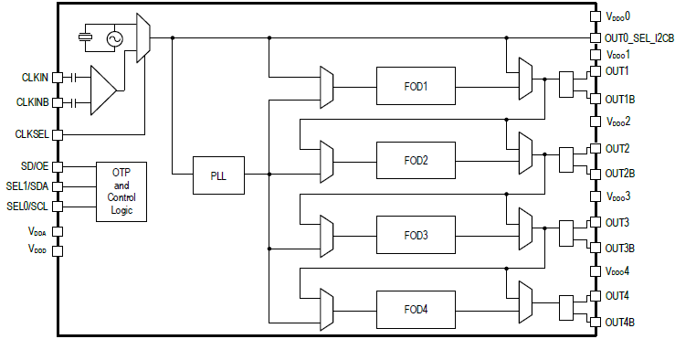
- 4 universal output pairs: LVPECL, LVDS, HCSL, or 8 LVCMOS outputs
- 4 independent frequencies with 0.001MHz–350MHz output range
- Reference output
- 1.8V/2.5V/3.3V core and output voltages
- 2 programmable I²C addresses allowing multiple devices to be used in the same system.
- Up to 4 different configuration sets in OTP non-volatile memory
- Supported by the Renesas IC Toolbox (RICBox) software tool
- Quick sampling and customization process supported by online form submission
- Internal crystal in package saves board space
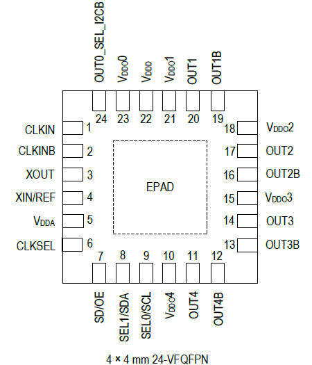
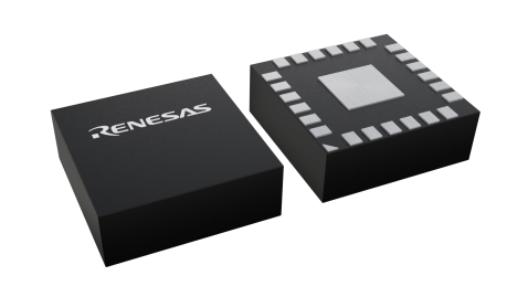
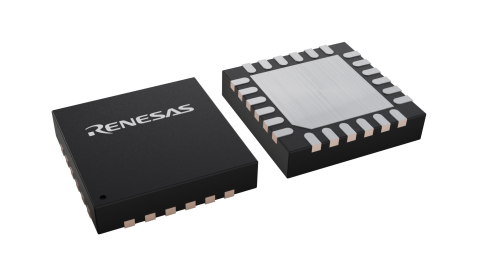
- 4mm x 4mm 24-VFQFPN package
- -40°C to +85°C operating temperature range
描述
The 5P49V6975 is a member of Renesas' VersaClock® 6E programmable clock generator family. The 5P49V6975 is intended for high-performance consumer, networking, industrial, computing, and data-communications applications. The reference clock can come from one of the two redundant clock inputs. A glitchless manual switchover function allows one of the redundant clocks to be selected during normal operation.
Configurations may be stored in on-chip One-Time Programmable (OTP) memory or changed using I²C& interface.
产品参数
| 属性 | 值 |
|---|---|
| Diff. Outputs | 4 |
| App Jitter Compliance | PCIe Gen1, PCIe Gen2, PCIe Gen3, PCIe Gen4, PCIe Gen5 |
| Outputs (#) | 5 |
| Output Type | LVCMOS, LVPECL, HCSL, LVDS |
| Output Freq Range (MHz) | 1 - 350 |
| Input Freq (MHz) | 1 - 350 |
| Inputs (#) | 1 |
| Input Type | Crystal, LVCMOS, LVPECL, LVDS, HCSL |
| Output Banks (#) | 4 |
| Core Voltage (V) | 1.8V, 2.5V, 3.3V |
| Output Voltage (V) | 1.8V, 2.5V, 3.3V |
| Product Category | VersaClock 6E, Low Jitter Clocks (<700 fs RMS), General Purpose Clocks, PCI Express Clocks, Programmable Clocks |
| Selection Criteria | <700 fs RM |
封装选项
| Pkg. Type | Pkg. Dimensions (mm) | Lead Count (#) | Pitch (mm) |
|---|---|---|---|
| LGA | 4.0 x 4.0 x 1.4 | 24 | 0.5 |
产品对比

应用
- Ethernet switch/router
- PCI Express 1.0/2.0/3.0/4.0 spread spectrum on
- PCI Express 1.0/2.0/3.0/4.0/5.0 spread spectrum off
- Broadcast video/audio timing
- Multi-function printer
- Processor and FPGA clocking
- Any-frequency clock conversion
- MSAN/DSLAM/PON
- Fiber Channel, SAN
- Telecom line cards
- Laser distance sensing