特性
- Low additive phase jitter RMS: 50fs
- Low skew outputs (50ps)
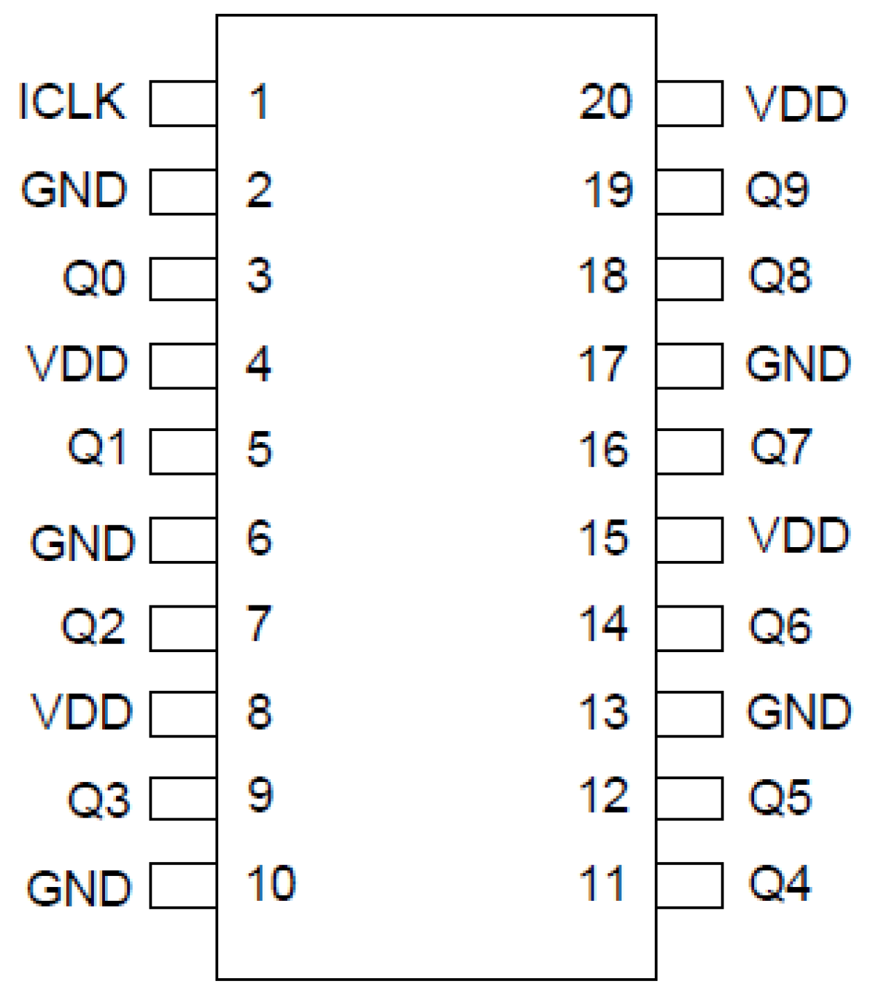
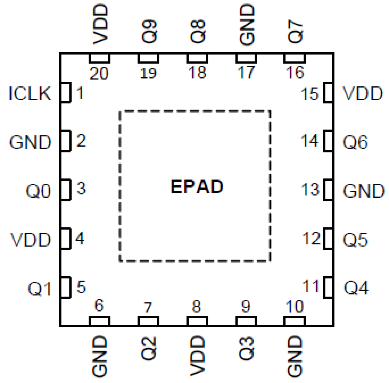
- Packaged in 20-pin TSSOP, SSOP, QSOP, and QFN packages, Pb (lead) free
- Operating voltages of 1.8V to 3.3V
- Input/Output clock frequency up to 200MHz
- Advanced, low-power CMOS process
- Extended temperature range: -40 °C to +105 °C
描述
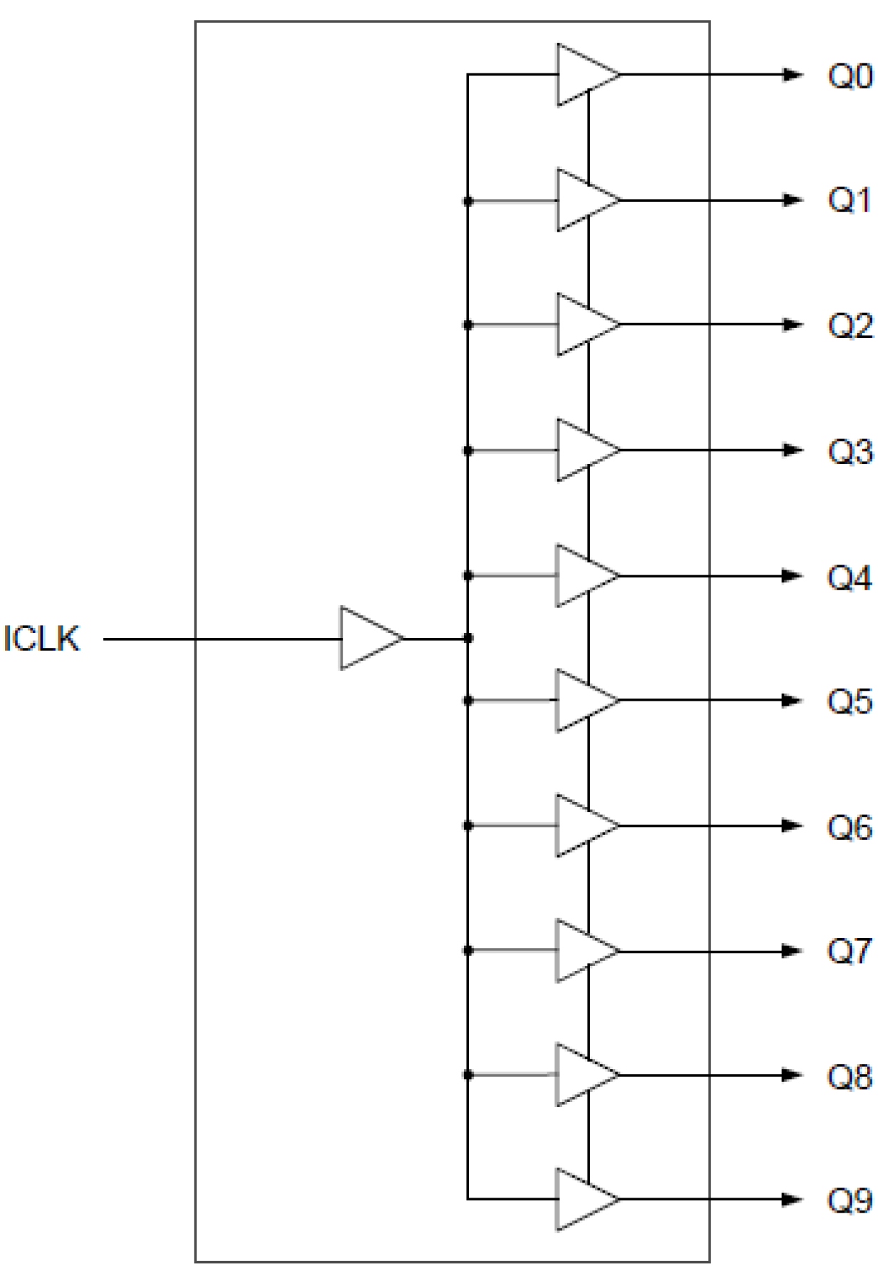
The 74FCT3807S is a low skew, single input to ten output, LVCMOS clock buffer that offers a best-in-class additive phase jitter of sub 50fs.
产品参数
| 属性 | 值 |
|---|---|
| Temp. Range (°C) | -40 to 85°C |
| Product Category | Clock Buffers & Drivers |
当前筛选条件


