
特性
- 2 differential LVHSTL outputs
- Selectable CLK0, CLK1 LVCMOS clock inputs
- CLK0 and CLK1 can accept the following input levels: LVCMOS or LVTTL
- Maximum output frequency: 350MHz
- Part-to-part skew: 350ps (maximum)
- Propagation delay: 1.3ns (maximum)
- VOH: 1.2V (maximum)
- 3.3V and 2.5V operating supply
- 0°C to 70°C ambient operating temperature
- Industrial temperature information available upon request
- Lead-Free package fully RoHS compliant
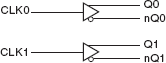
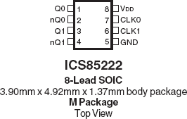
85222 - Block Diagram
描述
The 85222 is a Dual LVCMOS / LVTTL-to- Differential LVHSTL Translator. The 85222 has two single ended clock inputs. The single ended clock input accepts LVCMOS or LVTTL input levels and translates them to LVHSTL levels. The small outline 8-pin SOIC package makes this device ideal for applications where space, high performance and low power are important. For optimum performance, both output pairs need to be terminated, even if one output pair is unused.
| Part Number | Status | Samples | Stock | Package | Lead Count (#) | Carrier Type | Moisture Sensitivity Level (MSL) | Qty. per Reel (#) | Qty. per Carrier (#) | Pb (Lead) Free | Pb Free Category | Temp. Range (°C) |
|---|---|---|---|---|---|---|---|---|---|---|---|---|
| 85222AMLF | Obsolete | N/A | Out of Stock | SOIC | 8# | Tube | 1 | 0 | 97# | Yes | e3 Sn | 0 to 70°C |
| 85222AMLFT | Obsolete | N/A | Out of Stock | SOIC | 8# | Reel | 1 | 2500# | 0 | Yes | e3 Sn | 0 to 70°C |
加载中
请登录后开启订阅
- 应用说明英语PDF 495 KB 7WDXRDKU4E7E-5-57312 2014年5月12日
- 产品变更通告英语PDF 361 KB 7WDXRDKU4E7E-5-55130 2013年3月24日
- 产品变更通告英语PDF 439 KB 7WDXRDKU4E7E-5-56251 2013年10月11日
推荐文档 (1)
数据手册 (1)
No Results Found.
检查拼写
确保所有关键词拼写正确。
确保所有关键词拼写正确。
调整关键词
尝试使用更少、不同或更宽泛的词语来改变搜索结果。
尝试使用更少、不同或更宽泛的词语来改变搜索结果。
查看筛选器
如果您使用了筛选器,请考虑取消选择某些筛选器选项以扩大搜索结果。
如果您使用了筛选器,请考虑取消选择某些筛选器选项以扩大搜索结果。
需要帮助?
- 搜索我们丰富的知识库,帮助您解答常见问题
- 前往支持论坛,获取瑞萨电子技术专家和社群的帮助
- 应用说明英语PDF 495 KB 7WDXRDKU4E7E-5-57312 2014年5月12日查看更多 (8)
应用说明和白皮书 (8)
- 产品变更通告英语PDF 439 KB 7WDXRDKU4E7E-5-56251 2013年10月11日
- 产品变更通告英语PDF 361 KB 7WDXRDKU4E7E-5-55130 2013年3月24日
产品通告(产品变更、EOL 等) (3)
No Results Found.
检查拼写
确保所有关键词拼写正确。
确保所有关键词拼写正确。
调整关键词
尝试使用更少、不同或更宽泛的词语来改变搜索结果。
尝试使用更少、不同或更宽泛的词语来改变搜索结果。
查看筛选器
如果您使用了筛选器,请考虑取消选择某些筛选器选项以扩大搜索结果。
如果您使用了筛选器,请考虑取消选择某些筛选器选项以扩大搜索结果。
需要帮助?
- 搜索我们丰富的知识库,帮助您解答常见问题
- 前往支持论坛,获取瑞萨电子技术专家和社群的帮助
No Results Found.
检查拼写
确保所有关键词拼写正确。
确保所有关键词拼写正确。
调整关键词
尝试使用更少、不同或更宽泛的词语来改变搜索结果。
尝试使用更少、不同或更宽泛的词语来改变搜索结果。
查看筛选器
如果您使用了筛选器,请考虑取消选择某些筛选器选项以扩大搜索结果。
如果您使用了筛选器,请考虑取消选择某些筛选器选项以扩大搜索结果。
需要帮助?
- 搜索我们丰富的知识库,帮助您解答常见问题
- 前往支持论坛,获取瑞萨电子技术专家和社群的帮助
No Results Found.
检查拼写
确保所有关键词拼写正确。
确保所有关键词拼写正确。
调整关键词
尝试使用更少、不同或更宽泛的词语来改变搜索结果。
尝试使用更少、不同或更宽泛的词语来改变搜索结果。
查看筛选器
如果您使用了筛选器,请考虑取消选择某些筛选器选项以扩大搜索结果。
如果您使用了筛选器,请考虑取消选择某些筛选器选项以扩大搜索结果。
需要帮助?
- 搜索我们丰富的知识库,帮助您解答常见问题
- 前往支持论坛,获取瑞萨电子技术专家和社群的帮助
No Results Found.
检查拼写
确保所有关键词拼写正确。
确保所有关键词拼写正确。
调整关键词
尝试使用更少、不同或更宽泛的词语来改变搜索结果。
尝试使用更少、不同或更宽泛的词语来改变搜索结果。
查看筛选器
如果您使用了筛选器,请考虑取消选择某些筛选器选项以扩大搜索结果。
如果您使用了筛选器,请考虑取消选择某些筛选器选项以扩大搜索结果。
需要帮助?
- 搜索我们丰富的知识库,帮助您解答常见问题
- 前往支持论坛,获取瑞萨电子技术专家和社群的帮助
No Results Found.
检查拼写
确保所有关键词拼写正确。
确保所有关键词拼写正确。
调整关键词
尝试使用更少、不同或更宽泛的词语来改变搜索结果。
尝试使用更少、不同或更宽泛的词语来改变搜索结果。
查看筛选器
如果您使用了筛选器,请考虑取消选择某些筛选器选项以扩大搜索结果。
如果您使用了筛选器,请考虑取消选择某些筛选器选项以扩大搜索结果。
需要帮助?
- 搜索我们丰富的知识库,帮助您解答常见问题
- 前往支持论坛,获取瑞萨电子技术专家和社群的帮助
No Results Found.
检查拼写
确保所有关键词拼写正确。
确保所有关键词拼写正确。
调整关键词
尝试使用更少、不同或更宽泛的词语来改变搜索结果。
尝试使用更少、不同或更宽泛的词语来改变搜索结果。
查看筛选器
如果您使用了筛选器,请考虑取消选择某些筛选器选项以扩大搜索结果。
如果您使用了筛选器,请考虑取消选择某些筛选器选项以扩大搜索结果。
需要帮助?
- 搜索我们丰富的知识库,帮助您解答常见问题
- 前往支持论坛,获取瑞萨电子技术专家和社群的帮助
营销资料 (1)
No Results Found.
检查拼写
确保所有关键词拼写正确。
确保所有关键词拼写正确。
调整关键词
尝试使用更少、不同或更宽泛的词语来改变搜索结果。
尝试使用更少、不同或更宽泛的词语来改变搜索结果。
查看筛选器
如果您使用了筛选器,请考虑取消选择某些筛选器选项以扩大搜索结果。
如果您使用了筛选器,请考虑取消选择某些筛选器选项以扩大搜索结果。
需要帮助?
- 搜索我们丰富的知识库,帮助您解答常见问题
- 前往支持论坛,获取瑞萨电子技术专家和社群的帮助
No Results Found.
检查拼写
确保所有关键词拼写正确。
确保所有关键词拼写正确。
调整关键词
尝试使用更少、不同或更宽泛的词语来改变搜索结果。
尝试使用更少、不同或更宽泛的词语来改变搜索结果。
查看筛选器
如果您使用了筛选器,请考虑取消选择某些筛选器选项以扩大搜索结果。
如果您使用了筛选器,请考虑取消选择某些筛选器选项以扩大搜索结果。
需要帮助?
- 搜索我们丰富的知识库,帮助您解答常见问题
- 前往支持论坛,获取瑞萨电子技术专家和社群的帮助
加载中
筛选
当前筛选条件
软件与工具
按类型筛选
按供应商筛选
样例程序
按应用筛选
按功能筛选
按编译器筛选
按 IDE 筛选
模拟模型
Partner Solutions
No Results Found.
检查拼写
确保所有关键词拼写正确。
确保所有关键词拼写正确。
调整关键词
尝试使用更少、不同或更宽泛的词语来改变搜索结果。
尝试使用更少、不同或更宽泛的词语来改变搜索结果。
查看筛选器
如果您使用了筛选器,请考虑取消选择某些筛选器选项以扩大搜索结果。
如果您使用了筛选器,请考虑取消选择某些筛选器选项以扩大搜索结果。
需要帮助?
- 搜索我们丰富的知识库,帮助您解答常见问题
- 前往支持论坛,获取瑞萨电子技术专家和社群的帮助
No Results Found.
检查拼写
确保所有关键词拼写正确。
确保所有关键词拼写正确。
调整关键词
尝试使用更少、不同或更宽泛的词语来改变搜索结果。
尝试使用更少、不同或更宽泛的词语来改变搜索结果。
查看筛选器
如果您使用了筛选器,请考虑取消选择某些筛选器选项以扩大搜索结果。
如果您使用了筛选器,请考虑取消选择某些筛选器选项以扩大搜索结果。
需要帮助?
- 搜索我们丰富的知识库,帮助您解答常见问题
- 前往支持论坛,获取瑞萨电子技术专家和社群的帮助
No Results Found.
检查拼写
确保所有关键词拼写正确。
确保所有关键词拼写正确。
调整关键词
尝试使用更少、不同或更宽泛的词语来改变搜索结果。
尝试使用更少、不同或更宽泛的词语来改变搜索结果。
查看筛选器
如果您使用了筛选器,请考虑取消选择某些筛选器选项以扩大搜索结果。
如果您使用了筛选器,请考虑取消选择某些筛选器选项以扩大搜索结果。
需要帮助?
- 搜索我们丰富的知识库,帮助您解答常见问题
- 前往支持论坛,获取瑞萨电子技术专家和社群的帮助
模拟模型 (1)
No Results Found.
检查拼写
确保所有关键词拼写正确。
确保所有关键词拼写正确。
调整关键词
尝试使用更少、不同或更宽泛的词语来改变搜索结果。
尝试使用更少、不同或更宽泛的词语来改变搜索结果。
查看筛选器
如果您使用了筛选器,请考虑取消选择某些筛选器选项以扩大搜索结果。
如果您使用了筛选器,请考虑取消选择某些筛选器选项以扩大搜索结果。
需要帮助?
- 搜索我们丰富的知识库,帮助您解答常见问题
- 前往支持论坛,获取瑞萨电子技术专家和社群的帮助
