
| CAD 模型: | View CAD Model |
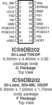
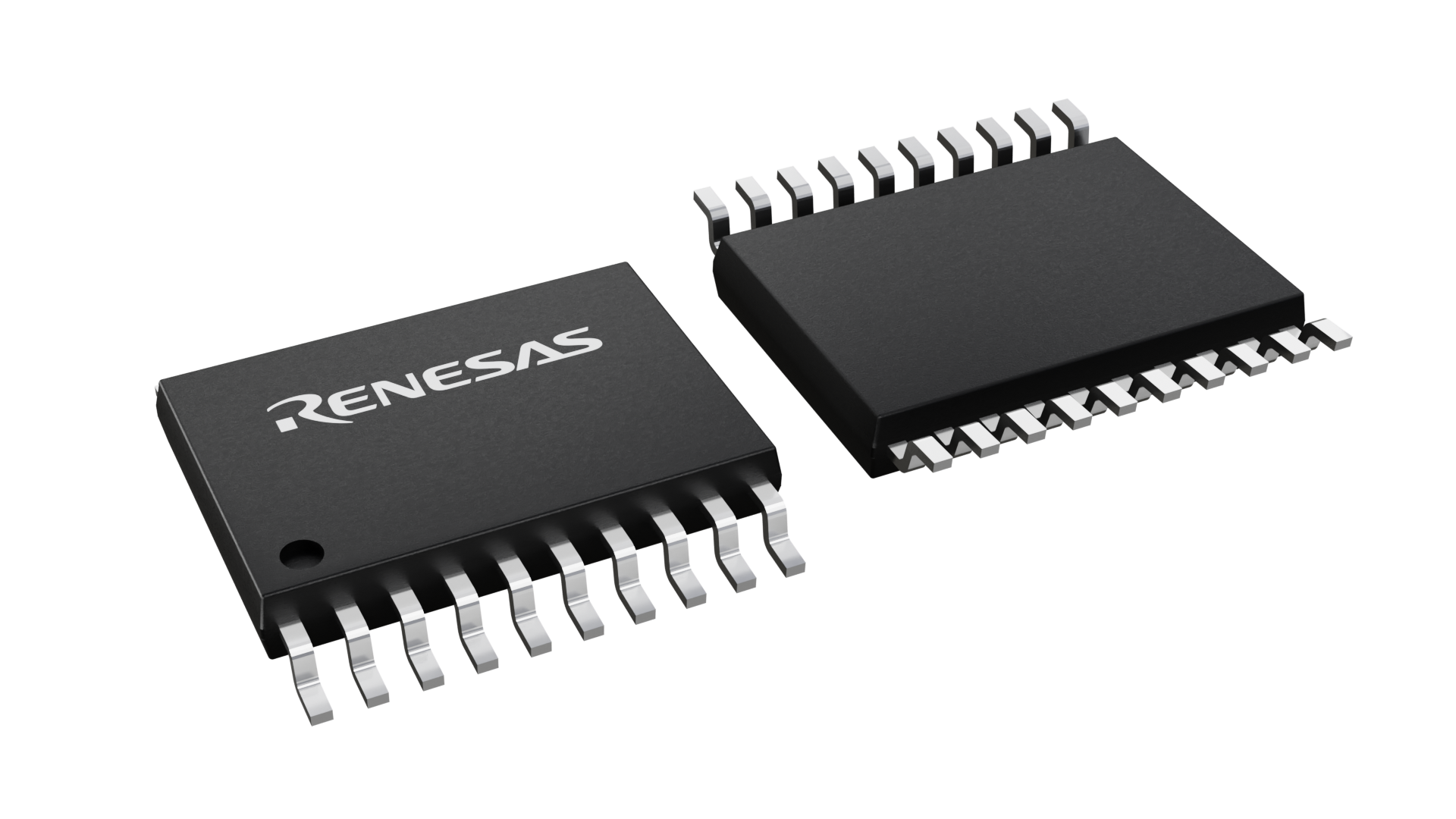
| Pkg. Type: | TSSOP |
| Pkg. Code: | PGG20 |
| Lead Count (#): | 20 |
| Pkg. Dimensions (mm): | 6.5 x 4.4 x 1.0 |
| Pitch (mm): | 0.65 |
| Pb (Lead) Free | Yes |
| Moisture Sensitivity Level (MSL) | 1 |
| ECCN (US) | |
| HTS (US) |
| Pkg. Type | TSSOP |
| Lead Count (#) | 20 |
| Pb (Lead) Free | Yes |
| Carrier Type | Tube |
| Advanced Features | Spread Spectrum |
| App Jitter Compliance | PCIe Gen1, PCIe Gen2 |
| C-C Jitter Max P-P (ps) | 50 |
| Core Voltage (V) | 3.3 |
| Feedback Input | No |
| Input Freq (MHz) | 90 - 140 |
| Input Type | HCSL, HSTL, LVDS, LVPECL, SSTL |
| Inputs (#) | 2 |
| Length (mm) | 6.5 |
| MOQ | 74 |
| Moisture Sensitivity Level (MSL) | 1 |
| Output Banks (#) | 2 |
| Output Freq Range (MHz) | 90 - 140 |
| Output Skew (ps) | 110 |
| Output Type | HCSL |
| Output Voltage (V) | 3.3 |
| Outputs (#) | 2 |
| Package Area (mm²) | 28.6 |
| Pb Free Category | e3 Sn |
| Phase Jitter Typ RMS (ps) | 2.42 |
| Pitch (mm) | 0.65 |
| Pkg. Dimensions (mm) | 6.5 x 4.4 x 1.0 |
| Prog. Clock | No |
| Qty. per Carrier (#) | 74 |
| Qty. per Reel (#) | 0 |
| Reference Output | No |
| Requires Terms and Conditions | Does not require acceptance of Terms and Conditions |
| Spread Spectrum | Yes |
| Tape & Reel | No |
| Temp. Range (°C) | 0 to 70°C |
| Thickness (mm) | 1 |
| Width (mm) | 4.4 |
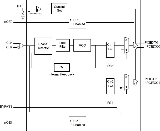
The 9DB202 is a high performance 1-to-2 Differential-to-HCSL Jitter Attenuator designed for use in PCI Express®™ systems. In some PCI Express®™ systems, such as those found in desktop PCs, the PCI Express®™ clocks are generated from a low bandwidth, high phase noise PLL frequency synthesizer. In these systems, a jitter-attenuating device may be necessary in order to reduce high frequency random and deterministic jitter components from the PLL synthesizer and from the system board. The 9DB202 has two PLL bandwidth modes. In low bandwidth mode, the PLL loop bandwidth is 500kHz. This setting offers the best jitter attenuation and is still high enough to pass a triangular input spread spectrum profile. In high bandwidth mode, the PLL bandwidth is at 1MHz and allows the PLL to pass more spread spectrum modulation. For serdes which have x10 reference multipliers instead of x12.5 multipliers, each of the two PCI Express®™ outputs (PCIEX0:1) can be set for 125MHz instead of 100MHz by configuring the appropriate frequency select pins (FS0:1).