特性
- Additive PCIe Gen 6 CC jitter < 18fs RMS (Fanout mode)
- PCIe Gen6 CC jitter < 100fs RMS (High-BW Zero-Delay Buffer (ZDB) mode)
- 6 Low Power HCSL (LP-HCSL) outputs eliminate 4 resistors per output pair
- Direct connection to 85Ω transmission lines
- Dedicated OE# pin for each output
- Spread spectrum tolerant
- Pin or SMBus configuration
- 3 selectable SMBus addresses
- SMBus interface not required for device operation
- Easy AC coupling to other logic families, see application note AN-891.
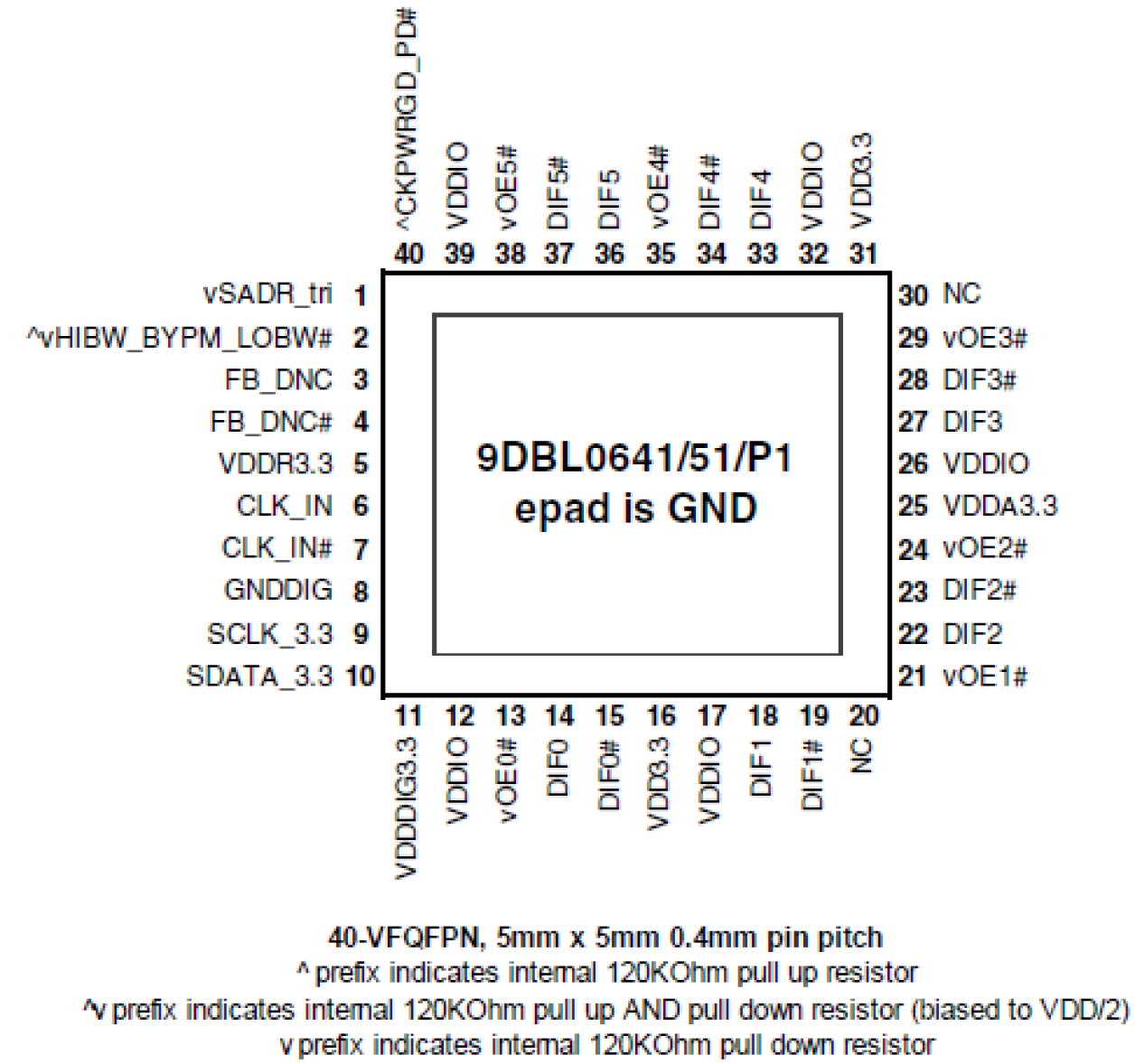
- Space-saving 40-pin 5mm × 5mm VFQFPN
描述
The 9DBL0651 6-output 3.3V PCIe zero-delay/fanout buffer supports PCIe Gen 1 through Gen 6 and both Common and Independent Reference Clock architectures.
For information regarding evaluation boards and material, please contact your local sales representative.
产品参数
| 属性 | 值 |
|---|---|
| Diff. Outputs | 6 |
| Diff. Output Signaling | LP-HCSL |
| Output Freq Range (MHz) | 1 - 200 |
| Diff. Inputs | 1 |
| Diff. Input Signaling | HCSL |
| Accepts Spread Spec Input | Yes |
| Power Consumption Typ (mW) | 149 |
| Supply Voltage (V) | 3.3 - 3.3 |
| Output Type | LP-HCSL |
| Diff. Termination Resistors | 0 |
| Package Area (mm²) | 25 |
| Battery Backup | No |
| Battery Seal | No |
| CPU Supervisory Function POR | No |
| Crystal Frequency Trimming | No |
| Frequency Out Pin | No |
| Inputs (#) | 1 |
| Input Freq (MHz) | 1 - 200 |
| Additive Phase Jitter Typ RMS (fs) | 300 |
| Function | Zero Delay Buffer |
| Input Type | HCSL |
| Output Banks (#) | 1 |
| Core Voltage (V) | 3.3 |
| Output Voltage (V) | 0.8 |
| Product Category | PCI Express Clocks |
封装选项
| Pkg. Type | Pkg. Dimensions (mm) | Lead Count (#) | Pitch (mm) |
|---|---|---|---|
| VFQFPN | 5.0 x 5.0 x 0.9 | 40 | 0.4 |
当前筛选条件


