特性
- PCIe Gen 1–5 compliant
- PCIe Gen 5 Common Clock jitter < 80fs RMS
- 284fs RMS typical phase jitter at 156.25MHz (12kHz to 20MHz)
- 2 programmable output pairs plus 1 LVCMOS REF outputs
- 1 integer output frequency per configuration
- 1MHz to 325MHz output frequency (LVDS or LP-HCSL)
- 1MHz to 200MHz output frequency (LVCMOS)
- 1.8V to 3.3V core VDD
- Individual 1.8V to 3.3V VDDO for each programmable output pair
- Supports HCSL, LVDS, and LVCMOS I/O standards
- Supports AC-coupled LVPECL and CML logic – See AN-891
- 3mm × 3mm 16-LGA packages with 50MHz integrated crystal option
- Supported by Timing Commander™ software


")


描述
The 9FGV1005 is a member of Renesas' PhiClock™ programmable clock generator family. The 9FGV1005 provides two copies of a single non-spread spectrum output frequency and one copy of the crystal reference input. Two select pins allow for hardware selection of the desired configuration, or two I²C bits all easy software selection of the desired configuration. The user may configure any one of the four OTP configurations as the default when operating in I²C mode. Four unique I²C addresses are available, allowing easy I²C access to multiple components.
试用自定义部件配置工具。
产品参数
| 属性 | 值 |
|---|---|
| Diff. Outputs | 2 |
| Diff. Output Signaling | LP-HCSL |
| Output Freq Range (MHz) | 50 - 50, 100 - 100, 125 - 125, 156.25 - 156.25, 161.1328125 - 161.1328125, 312.5 - 312.5, 322.265625 - 322.265625, 156.25 - 156.25 |
| Accepts Spread Spec Input | No |
| Power Consumption Typ (mW) | 100 |
| Supply Voltage (V) | 1.8 - 1.8, 3.3 - 3.3 |
| Output Type | LP-HCSL |
| Xtal Freq (MHz) | 25 - 25, 39.0625 - 39.0625, 50 - 50 |
| Package Area (mm²) | 25 |
| Battery Backup | No |
| Battery Seal | No |
| CPU Supervisory Function POR | No |
| Crystal Frequency Trimming | No |
| Frequency Out Pin | No |
| Inputs (#) | 1 |
| Input Freq (MHz) | 25 - 25, 39.0625 - 39.0625, 50 - 50 |
| Function | Generator |
| Input Type | Crystal, LVCMOS |
| Output Banks (#) | 1 |
| Core Voltage (V) | 1.8, 3.3 |
| Output Voltage (V) | 1.8, 3.3 |
| Product Category | PhiClock, PCI Express Clocks, Programmable Clocks |
封装选项
| Pkg. Type | Pkg. Dimensions (mm) | Lead Count (#) | Pitch (mm) |
|---|---|---|---|
| LGA | 3.0 x 3.0 x 1.1 | 16 | 0.5 |
试用自定义部件配置工具。
| Part Number | Status | Samples | Longevity | Stock | Package | Budgetary Price (USD) | Lead Count (#) | Carrier Type | Moisture Sensitivity Level (MSL) | Phase Jitter Typ RMS (ps) | Input Freq (MHz) | Xtal Freq (MHz) | Core Voltage (V) | Diff. Output Signaling | Output Freq Range (MHz) | Output Type | Output Voltage (V) | Supply Voltage (V) | Advanced Features | App Jitter Compliance | Input Type | Outputs (#) | Output Impedance | Power Consumption Typ (mW) | Prog. Clock | Qty. per Reel (#) | Spread Spectrum | Qty. per Carrier (#) | Xtal Inputs (#) | Pb (Lead) Free | Pb Free Category | Temp. Range (°C) | Country of Assembly | Country of Wafer Fabrication |
|---|---|---|---|---|---|---|---|---|---|---|---|---|---|---|---|---|---|---|---|---|---|---|---|---|---|---|---|---|---|---|---|---|---|---|
| 9FGV1005C001LTGI | Active | Available | 2040 Apr | Out of Stock | LGA | 16# | Tray | 3 | 0.267ps | 25 - 25 | 25 - 25 | 3.3V | LP-HCSL | 50 - 50, 100 - 100, 125 - 125, 156.25 - 156.25 | LP-HCSL | 3.3V | 3.3 - 3.3 | Programmable Clock | PCIe Gen1, PCIe Gen2, PCIe Gen3, PCIe Gen4, PCIe Gen5 | Crystal, LVCMOS | 2# | 100 | 100mW | Yes | 0 | No | 490# | 1# | Yes | e4 Au | -40 to 85°C | |||
| 9FGV1005C001LTGI8 | Active | N/A | 2040 Apr | Out of Stock | LGA | 16# | Reel | 3 | 0.267ps | 25 - 25 | 25 - 25 | 3.3V | LP-HCSL | 50 - 50, 100 - 100, 125 - 125, 156.25 - 156.25 | LP-HCSL | 3.3V | 3.3 - 3.3 | Programmable Clock | PCIe Gen1, PCIe Gen2, PCIe Gen3, PCIe Gen4, PCIe Gen5 | Crystal, LVCMOS | 2# | 100 | 100mW | Yes | 3000# | No | 0 | 1# | Yes | e4 Au | -40 to 85°C | |||
| 9FGV1005C002LTGI | Active | Available | 2040 Apr | Out of Stock | LGA | 16# | Tray | 3 | 0.304ps | 25 - 25 | 25 - 25 | 1.8V | LP-HCSL | 50 - 50, 100 - 100, 125 - 125, 156.25 - 156.25 | LP-HCSL | 1.8V | 1.8 - 1.8 | Programmable Clock | PCIe Gen1, PCIe Gen2, PCIe Gen3, PCIe Gen4, PCIe Gen5 | Crystal, LVCMOS | 2# | 100 | 100mW | Yes | 0 | No | 490# | 1# | Yes | e4 Au | -40 to 85°C | |||
| 9FGV1005C002LTGI8 | Active | N/A | 2040 Apr | Out of Stock | LGA | 16# | Reel | 3 | 0.304ps | 25 - 25 | 25 - 25 | 1.8V | LP-HCSL | 50 - 50, 100 - 100, 125 - 125, 156.25 - 156.25 | LP-HCSL | 1.8V | 1.8 - 1.8 | Programmable Clock | PCIe Gen1, PCIe Gen2, PCIe Gen3, PCIe Gen4, PCIe Gen5 | Crystal, LVCMOS | 2# | 100 | 100mW | Yes | 3000# | No | 0 | 1# | Yes | e4 Au | -40 to 85°C | |||
| 9FGV1005C011LTGI | Active | Available | 2040 Apr | Out of Stock | LGA | 16# | Tray | 3 | 0.234ps | 39.0625 - 39.0625 | 39.0625 - 39.0625 | 3.3V | LP-HCSL | 161.1328125 - 161.1328125, 312.5 - 312.5, 322.265625 - 322.265625, 156.25 - 156.25 | LP-HCSL | 3.3V | 3.3 - 3.3 | Programmable Clock | PCIe Gen1, PCIe Gen2, PCIe Gen3, PCIe Gen4, PCIe Gen5 | Crystal, LVCMOS | 2# | 100 | 100mW | Yes | 0 | No | 490# | 1# | Yes | e4 Au | -40 to 85°C | |||
| 9FGV1005C011LTGI8 | Active | N/A | 2040 Apr | Out of Stock | LGA | 16# | Reel | 3 | 0.234ps | 39.0625 - 39.0625 | 39.0625 - 39.0625 | 3.3V | LP-HCSL | 161.1328125 - 161.1328125, 312.5 - 312.5, 322.265625 - 322.265625, 156.25 - 156.25 | LP-HCSL | 3.3V | 3.3 - 3.3 | Programmable Clock | PCIe Gen1, PCIe Gen2, PCIe Gen3, PCIe Gen4, PCIe Gen5 | Crystal, LVCMOS | 2# | 100 | 100mW | Yes | 3000# | No | 0 | 1# | Yes | e4 Au | -40 to 85°C | |||
| 9FGV1005C012LTGI | Active | Available | 2040 Apr | Out of Stock | LGA | 16# | Tray | 3 | 0.262ps | 39.0625 - 39.0625 | 39.0625 - 39.0625 | 1.8V | LP-HCSL | 161.1328125 - 161.1328125, 312.5 - 312.5, 322.265625 - 322.265625, 156.25 - 156.25 | LP-HCSL | 1.8V | 1.8 - 1.8 | Programmable Clock | PCIe Gen1, PCIe Gen2, PCIe Gen3, PCIe Gen4, PCIe Gen5 | Crystal, LVCMOS | 2# | 100 | 100mW | Yes | 0 | No | 490# | 1# | Yes | e4 Au | -40 to 85°C | |||
| 9FGV1005C012LTGI8 | Active | N/A | 2040 Apr | Out of Stock | LGA | 16# | Reel | 3 | 0.262ps | 39.0625 - 39.0625 | 39.0625 - 39.0625 | 1.8V | LP-HCSL | 161.1328125 - 161.1328125, 312.5 - 312.5, 322.265625 - 322.265625, 156.25 - 156.25 | LP-HCSL | 1.8V | 1.8 - 1.8 | Programmable Clock | PCIe Gen1, PCIe Gen2, PCIe Gen3, PCIe Gen4, PCIe Gen5 | Crystal, LVCMOS | 2# | 100 | 100mW | Yes | 3000# | No | 0 | 1# | Yes | e4 Au | -40 to 85°C | |||
| 9FGV1005CQ505LTGI | Active | Available | 2040 Apr | In Stock | LGA | 1ku | $2.74 | 16# | Tray | 3 | 0.223ps | 50 - 50 | 50 - 50 | 3.3V | LP-HCSL | 50 - 50, 100 - 100, 125 - 125, 156.25 - 156.25 | LP-HCSL | 3.3V | 3.3 - 3.3 | Programmable Clock | PCIe Gen1, PCIe Gen2, PCIe Gen3, PCIe Gen4, PCIe Gen5 | Crystal, LVCMOS | 2# | 100 | 100mW | Yes | 0 | No | 490# | 1# | Yes | e4 Au | -40 to 85°C | TAIWAN | SINGAPORE |
| 9FGV1005CQ505LTGI8 | Active | N/A | 2040 Apr | Out of Stock | LGA | 1ku | $2.74 | 16# | Reel | 3 | 0.223ps | 50 - 50 | 50 - 50 | 3.3V | LP-HCSL | 50 - 50, 100 - 100, 125 - 125, 156.25 - 156.25 | LP-HCSL | 3.3V | 3.3 - 3.3 | Programmable Clock | PCIe Gen1, PCIe Gen2, PCIe Gen3, PCIe Gen4, PCIe Gen5 | Crystal, LVCMOS | 2# | 100 | 100mW | Yes | 3000# | No | 0 | 1# | Yes | e4 Au | -40 to 85°C | TAIWAN | SINGAPORE |
| 9FGV1005CQ506LTGI | Active | Available | 2040 Apr | In Stock | LGA | 1ku | $2.74 | 16# | Tray | 3 | 0.273ps | 50 - 50 | 50 - 50 | 1.8V | LP-HCSL | 50 - 50, 100 - 100, 125 - 125, 156.25 - 156.25 | LP-HCSL | 1.8V | 1.8 - 1.8 | Programmable Clock | PCIe Gen1, PCIe Gen2, PCIe Gen3, PCIe Gen4, PCIe Gen5 | Crystal, LVCMOS | 2# | 100 | 100mW | Yes | 0 | No | 490# | 1# | Yes | e4 Au | -40 to 85°C | TAIWAN | SINGAPORE |
| 9FGV1005CQ506LTGI8 | Active | N/A | 2040 Apr | Out of Stock | LGA | 1ku | $2.74 | 16# | Reel | 3 | 0.273ps | 50 - 50 | 50 - 50 | 1.8V | LP-HCSL | 50 - 50, 100 - 100, 125 - 125, 156.25 - 156.25 | LP-HCSL | 1.8V | 1.8 - 1.8 | Programmable Clock | PCIe Gen1, PCIe Gen2, PCIe Gen3, PCIe Gen4, PCIe Gen5 | Crystal, LVCMOS | 2# | 100 | 100mW | Yes | 3000# | No | 0 | 1# | Yes | e4 Au | -40 to 85°C | TAIWAN | SINGAPORE |
| 9FGV1005A000LTGI | Obsolete | N/A | Out of Stock | LGA | 16# | Tray | 3 | 0.246ps | 8 - 50 | 8 - 50 | 1.8V, 2.5V, 3.3V | LP-HCSL, LVDS | 10 - 325 | LP-HCSL, LVCMOS, LVDS | 1.8V, 2.5V, 3.3V | 1.8 - 1.8, 2.5 - 2.5, 3.3 - 3.3 | Reference Output, Spread Spectrum, Programmable Clock | PCIe Gen1, PCIe Gen2, PCIe Gen3, PCIe Gen4 | Crystal, LVCMOS | 3# | 85, 100 | 100mW | No | 0 | Yes | 490# | 1# | Yes | e4 Au | -40 to 85°C | ||||
| 9FGV1005A000LTGI8 | Obsolete | N/A | Out of Stock | LGA | 16# | Reel | 3 | 0.246ps | 8 - 50 | 8 - 50 | 1.8V, 2.5V, 3.3V | LP-HCSL, LVDS | 10 - 325 | LP-HCSL, LVCMOS, LVDS | 1.8V, 2.5V, 3.3V | 1.8 - 1.8, 2.5 - 2.5, 3.3 - 3.3 | Reference Output, Spread Spectrum, Programmable Clock | PCIe Gen1, PCIe Gen2, PCIe Gen3, PCIe Gen4 | Crystal, LVCMOS | 3# | 85, 100 | 100mW | No | 3000# | Yes | 0 | 1# | Yes | e4 Au | -40 to 85°C | ||||
| 9FGV1005A001LTGI | NRND | Available | In Stock | LGA | 16# | Tray | 3 | 0.246ps | 25 - 25 | 25 - 25 | 3.3V | LP-HCSL | 50 - 50, 100 - 100, 125 - 125, 156.25 - 156.25 | LP-HCSL | 3.3V | 1.8 - 1.8, 2.5 - 2.5, 3.3 - 3.3 | Programmable Clock | PCIe Gen1, PCIe Gen2, PCIe Gen3, PCIe Gen4 | Crystal, LVCMOS | 2# | 100 | 125mW | No | 0 | No | 490# | 1# | Yes | e4 Au | -40 to 85°C | ||||
| 9FGV1005A001LTGI8 | NRND | N/A | Out of Stock | LGA | 16# | Reel | 3 | 0.246ps | 25 - 25 | 25 - 25 | 3.3V | LP-HCSL | 50 - 50, 100 - 100, 125 - 125, 156.25 - 156.25 | LP-HCSL | 3.3V | 1.8 - 1.8, 2.5 - 2.5, 3.3 - 3.3 | Programmable Clock | PCIe Gen1, PCIe Gen2, PCIe Gen3, PCIe Gen4 | Crystal, LVCMOS | 2# | 100 | 125mW | No | 3000# | No | 0 | 1# | Yes | e4 Au | -40 to 85°C | ||||
| 9FGV1005A002LTGI | Obsolete | N/A | Out of Stock | LGA | 16# | Tray | 3 | 0.246ps | 25 - 25 | 25 - 25 | 1.8V | LP-HCSL | 50 - 50, 100 - 100, 125 - 125, 156.25 - 156.25 | LP-HCSL | 1.8V | 1.8 - 1.8, 2.5 - 2.5, 3.3 - 3.3 | Programmable Clock | PCIe Gen1, PCIe Gen2, PCIe Gen3, PCIe Gen4 | Crystal, LVCMOS | 2# | 100 | 100mW | No | 0 | No | 490# | 1# | Yes | e4 Au | -40 to 85°C | ||||
| 9FGV1005A002LTGI8 | Obsolete | N/A | Out of Stock | LGA | 16# | Reel | 3 | 0.246ps | 25 - 25 | 25 - 25 | 1.8V | LP-HCSL | 50 - 50, 100 - 100, 125 - 125, 156.25 - 156.25 | LP-HCSL | 1.8V | 1.8 - 1.8, 2.5 - 2.5, 3.3 - 3.3 | Programmable Clock | PCIe Gen1, PCIe Gen2, PCIe Gen3, PCIe Gen4 | Crystal, LVCMOS | 2# | 100 | 100mW | No | 3000# | No | 0 | 1# | Yes | e4 Au | -40 to 85°C | ||||
| 9FGV1005A003LTGI | Obsolete | N/A | Out of Stock | LGA | 16# | Tray | 3 | 0.291ps | 25 - 25 | 25 - 25 | 3.3V | LVDS | 50 - 50, 100 - 100, 125 - 125, 156.25 - 156.25 | LVDS | 3.3V | 1.8 - 1.8, 2.5 - 2.5, 3.3 - 3.3 | Programmable Clock | PCIe Gen1, PCIe Gen2, PCIe Gen3, PCIe Gen4 | Crystal, LVCMOS | 2# | 100 | 125mW | No | 0 | No | 490# | 1# | Yes | e4 Au | -40 to 85°C | ||||
| 9FGV1005A003LTGI8 | Obsolete | N/A | Out of Stock | LGA | 16# | Reel | 3 | 0.246ps | 25 - 25 | 25 - 25 | 3.3V | LVDS | 50 - 50, 100 - 100, 125 - 125, 156.25 - 156.25 | LVDS | 3.3V | 1.8 - 1.8, 2.5 - 2.5, 3.3 - 3.3 | Programmable Clock | PCIe Gen1, PCIe Gen2, PCIe Gen3, PCIe Gen4 | Crystal, LVCMOS | 2# | 100 | 125mW | No | 3000# | No | 0 | 1# | Yes | e4 Au | -40 to 85°C | ||||
| 9FGV1005A004LTGI | Obsolete | N/A | Out of Stock | LGA | 16# | Tray | 3 | 0.246ps | 25 - 25 | 25 - 25 | 1.8V | LVDS | 50 - 50, 100 - 100, 125 - 125, 156.25 - 156.25 | LVDS | 1.8V | 1.8 - 1.8, 2.5 - 2.5, 3.3 - 3.3 | Programmable Clock | PCIe Gen1, PCIe Gen2, PCIe Gen3, PCIe Gen4 | Crystal, LVCMOS | 2# | 100 | 100mW | No | 0 | No | 490# | 1# | Yes | e4 Au | -40 to 85°C | ||||
| 9FGV1005A004LTGI8 | Obsolete | N/A | Out of Stock | LGA | 16# | Reel | 3 | 0.246ps | 25 - 25 | 25 - 25 | 1.8V | LVDS | 50 - 50, 100 - 100, 125 - 125, 156.25 - 156.25 | LVDS | 1.8V | 1.8 - 1.8, 2.5 - 2.5, 3.3 - 3.3 | Programmable Clock | PCIe Gen1, PCIe Gen2, PCIe Gen3, PCIe Gen4 | Crystal, LVCMOS | 2# | 100 | 100mW | No | 3000# | No | 0 | 1# | Yes | e4 Au | -40 to 85°C | ||||
| 9FGV1005Q500LTGI | Obsolete | N/A | Out of Stock | LGA | 16# | Tray | 3 | 0.246ps | 8 - 50 | 50 - 50 | 1.8V, 2.5V, 3.3V | LP-HCSL, LVDS | 10 - 325 | LP-HCSL, LVCMOS, LVDS | 1.8V, 2.5V, 3.3V | 1.8 - 1.8, 2.5 - 2.5, 3.3 - 3.3 | Reference Output, Spread Spectrum, Programmable Clock | PCIe Gen1, PCIe Gen2, PCIe Gen3, PCIe Gen4 | Crystal, LVCMOS | 3# | 85, 100 | 100mW | No | 0 | Yes | 490# | 1# | Yes | e4 Au | -40 to 85°C | ||||
| 9FGV1005Q500LTGI8 | Obsolete | N/A | Out of Stock | LGA | 16# | Reel | 3 | 0.246ps | 8 - 50 | 50 - 50 | 1.8V, 2.5V, 3.3V | LP-HCSL, LVDS | 10 - 325 | LP-HCSL, LVCMOS, LVDS | 1.8V, 2.5V, 3.3V | 1.8 - 1.8, 2.5 - 2.5, 3.3 - 3.3 | Reference Output, Spread Spectrum, Programmable Clock | PCIe Gen1, PCIe Gen2, PCIe Gen3, PCIe Gen4 | Crystal, LVCMOS | 3# | 85, 100 | 100mW | No | 3000# | Yes | 0 | 1# | Yes | e4 Au | -40 to 85°C | ||||
| 9FGV1005Q505LTGI | Obsolete | N/A | Out of Stock | LGA | 16# | Tray | 3 | 0.246ps | 50 - 50 | 50 - 50 | 3.3V | LP-HCSL | 50 - 50, 100 - 100, 125 - 125, 156.25 - 156.25 | LP-HCSL | 3.3V | 1.8 - 1.8, 2.5 - 2.5, 3.3 - 3.3 | Programmable Clock | PCIe Gen1, PCIe Gen2, PCIe Gen3, PCIe Gen4 | Crystal (integrated) | 2# | 100 | 125mW | No | 0 | No | 490# | 0 | Yes | e4 Au | -40 to 85°C | ||||
| 9FGV1005Q505LTGI8 | Obsolete | N/A | Out of Stock | LGA | 16# | Reel | 3 | 0.267ps | 50 - 50 | 50 - 50 | 3.3V | LP-HCSL | 50 - 50, 100 - 100, 125 - 125, 156.25 - 156.25 | LP-HCSL | 3.3V | 1.8 - 1.8, 2.5 - 2.5, 3.3 - 3.3 | Programmable Clock | PCIe Gen1, PCIe Gen2, PCIe Gen3, PCIe Gen4 | Crystal (integrated) | 2# | 100 | 125mW | No | 3000# | No | 0 | 0 | Yes | e4 Au | -40 to 85°C | ||||
| 9FGV1005Q506LTGI | Obsolete | N/A | Out of Stock | LGA | 16# | Tray | 3 | 0.246ps | 50 - 50 | 50 - 50 | 1.8V | LP-HCSL | 50 - 50, 100 - 100, 125 - 125, 156.25 - 156.25 | LP-HCSL | 1.8V | 1.8 - 1.8, 2.5 - 2.5, 3.3 - 3.3 | Programmable Clock | PCIe Gen1, PCIe Gen2, PCIe Gen3, PCIe Gen4 | Crystal (integrated) | 2# | 100 | 100mW | No | 0 | No | 490# | 0 | Yes | e4 Au | -40 to 85°C | ||||
| 9FGV1005Q506LTGI8 | Obsolete | N/A | Out of Stock | LGA | 16# | Reel | 3 | 0.304ps | 50 - 50 | 50 - 50 | 1.8V | LP-HCSL | 50 - 50, 100 - 100, 125 - 125, 156.25 - 156.25 | LP-HCSL | 1.8V | 1.8 - 1.8, 2.5 - 2.5, 3.3 - 3.3 | Programmable Clock | PCIe Gen1, PCIe Gen2, PCIe Gen3, PCIe Gen4 | Crystal (integrated) | 2# | 100 | 100mW | No | 3000# | No | 0 | 0 | Yes | e4 Au | -40 to 85°C | ||||
| 9FGV1005Q507LTGI | Obsolete | N/A | Out of Stock | LGA | 16# | Tray | 3 | 0.291ps | 50 - 50 | 50 - 50 | 3.3V | LVDS | 50 - 50, 100 - 100, 125 - 125, 156.25 - 156.25 | LVDS | 3.3V | 1.8 - 1.8, 2.5 - 2.5, 3.3 - 3.3 | Programmable Clock | PCIe Gen1, PCIe Gen2, PCIe Gen3, PCIe Gen4 | Crystal (integrated) | 2# | 100 | 125mW | No | 0 | No | 490# | 0 | Yes | e4 Au | -40 to 85°C | ||||
| 9FGV1005Q507LTGI8 | Obsolete | N/A | Out of Stock | LGA | 16# | Reel | 3 | 0.246ps | 50 - 50 | 50 - 50 | 3.3V | LVDS | 50 - 50, 100 - 100, 125 - 125, 156.25 - 156.25 | LVDS | 3.3V | 1.8 - 1.8, 2.5 - 2.5, 3.3 - 3.3 | Programmable Clock | PCIe Gen1, PCIe Gen2, PCIe Gen3, PCIe Gen4 | Crystal (integrated) | 2# | 100 | 125mW | No | 3000# | No | 0 | 0 | Yes | e4 Au | -40 to 85°C | ||||
| 9FGV1005Q508LTGI | Obsolete | N/A | Out of Stock | LGA | 16# | Tray | 3 | 0.246ps | 50 - 50 | 50 - 50 | 1.8V | LVDS | 50 - 50, 100 - 100, 125 - 125, 156.25 - 156.25 | LVDS | 1.8V | 1.8 - 1.8, 2.5 - 2.5, 3.3 - 3.3 | Programmable Clock | PCIe Gen1, PCIe Gen2, PCIe Gen3, PCIe Gen4 | Crystal (integrated) | 2# | 100 | 100mW | No | 0 | No | 490# | 0 | Yes | e4 Au | -40 to 85°C | ||||
| 9FGV1005Q508LTGI8 | Obsolete | N/A | Out of Stock | LGA | 16# | Reel | 3 | 0.246ps | 50 - 50 | 50 - 50 | 1.8V | LVDS | 50 - 50, 100 - 100, 125 - 125, 156.25 - 156.25 | LVDS | 1.8V | 1.8 - 1.8, 2.5 - 2.5, 3.3 - 3.3 | Programmable Clock | PCIe Gen1, PCIe Gen2, PCIe Gen3, PCIe Gen4 | Crystal (integrated) | 2# | 100 | 100mW | No | 3000# | No | 0 | 0 | Yes | e4 Au | -40 to 85°C |
- 应用说明英语PDF 1.53 MB R31AN0034EU0102 Rev.1.02 2025年10月21日AI 生成的摘要: PLL loop filter design involves selecting component values to ensure stable operation and optimized phase noise. The loop bandwidth depends on parameters like charge pump current, VCO gain, and feedback divider. Second and third order passive loop filters are common, with specific calculations for cutoff, zero, and pole frequencies guiding component selection. Proper tuning of loop bandwidth enhances PLL stability and phase noise performance, demonstrated through lab experiments and calculation examples.
- 应用说明英语PDF 431 KB 7WDXRDKU4E7E-5-59216 2023年12月06日
- 应用说明英语PDF 256 KB 2021年7月05日AI 生成的摘要: The document explains methods to generate a 1.2V LVCMOS signal from a 1.8V LVCMOS output by attenuating the amplitude without lowering the driver voltage. It details typical LVCMOS driver and receiver configurations, impedance matching using source termination, and the use of a parallel resistor at the receiver input to reduce signal amplitude. Simulation and measurement results demonstrate that adding a parallel resistor effectively lowers the voltage to 1.2V while maintaining signal integrity and minimal impact on jitter and frequency. This approach supports flexible amplitude adjustment for various low-voltage LVCMOS requirements in clock signal applications.
- 应用说明英语PDF 134 KB 2020年6月18日AI 生成的摘要: Various methods to drive crystal input pins or differential receivers are detailed, including direct LVCMOS clock driving with impedance matching via series resistors to prevent signal distortion. The document covers configurations for single-ended HCSL inputs, LVPECL, LVDS, and coaxial inputs, emphasizing proper voltage levels, coupling methods, and termination resistors. It also explains layout considerations for crystal or clock oscillator inputs, load capacitor variations, and level shifting techniques for different voltage domains. Practical component values and connection guidelines ensure signal integrity and compatibility across multiple interface types.
推荐文档 (1)
数据手册 (7)
- 手册 - 软件英语PDF 293 KB 7WDXRDKU4E7E-5-62423 2018年3月07日
- 手册 - 软件英语PDF 1.5 MB 7WDXRDKU4E7E-5-62522 2018年2月23日
- 手册 - 软件英语PDF 401 KB 7WDXRDKU4E7E-5-62508 2017年11月27日
手册和指南 (3)
- 应用说明英语PDF 1.53 MB R31AN0034EU0102 Rev.1.02 2025年10月21日AI 生成的摘要: PLL loop filter design involves selecting component values to ensure stable operation and optimized phase noise. The loop bandwidth depends on parameters like charge pump current, VCO gain, and feedback divider. Second and third order passive loop filters are common, with specific calculations for cutoff, zero, and pole frequencies guiding component selection. Proper tuning of loop bandwidth enhances PLL stability and phase noise performance, demonstrated through lab experiments and calculation examples.
- 应用说明英语PDF 431 KB 7WDXRDKU4E7E-5-59216 2023年12月06日
- 应用说明英语PDF 256 KB 2021年7月05日AI 生成的摘要: The document explains methods to generate a 1.2V LVCMOS signal from a 1.8V LVCMOS output by attenuating the amplitude without lowering the driver voltage. It details typical LVCMOS driver and receiver configurations, impedance matching using source termination, and the use of a parallel resistor at the receiver input to reduce signal amplitude. Simulation and measurement results demonstrate that adding a parallel resistor effectively lowers the voltage to 1.2V while maintaining signal integrity and minimal impact on jitter and frequency. This approach supports flexible amplitude adjustment for various low-voltage LVCMOS requirements in clock signal applications.查看更多 (19)
应用说明和白皮书 (19)
产品通告(产品变更、EOL 等) (2)
No Results Found.
确保所有关键词拼写正确。
尝试使用更少、不同或更宽泛的词语来改变搜索结果。
如果您使用了筛选器,请考虑取消选择某些筛选器选项以扩大搜索结果。
- 搜索我们丰富的知识库,帮助您解答常见问题
- 前往支持论坛,获取瑞萨电子技术专家和社群的帮助
No Results Found.
确保所有关键词拼写正确。
尝试使用更少、不同或更宽泛的词语来改变搜索结果。
如果您使用了筛选器,请考虑取消选择某些筛选器选项以扩大搜索结果。
- 搜索我们丰富的知识库,帮助您解答常见问题
- 前往支持论坛,获取瑞萨电子技术专家和社群的帮助
No Results Found.
确保所有关键词拼写正确。
尝试使用更少、不同或更宽泛的词语来改变搜索结果。
如果您使用了筛选器,请考虑取消选择某些筛选器选项以扩大搜索结果。
- 搜索我们丰富的知识库,帮助您解答常见问题
- 前往支持论坛,获取瑞萨电子技术专家和社群的帮助
No Results Found.
确保所有关键词拼写正确。
尝试使用更少、不同或更宽泛的词语来改变搜索结果。
如果您使用了筛选器,请考虑取消选择某些筛选器选项以扩大搜索结果。
- 搜索我们丰富的知识库,帮助您解答常见问题
- 前往支持论坛,获取瑞萨电子技术专家和社群的帮助
No Results Found.
确保所有关键词拼写正确。
尝试使用更少、不同或更宽泛的词语来改变搜索结果。
如果您使用了筛选器,请考虑取消选择某些筛选器选项以扩大搜索结果。
- 搜索我们丰富的知识库,帮助您解答常见问题
- 前往支持论坛,获取瑞萨电子技术专家和社群的帮助
No Results Found.
确保所有关键词拼写正确。
尝试使用更少、不同或更宽泛的词语来改变搜索结果。
如果您使用了筛选器,请考虑取消选择某些筛选器选项以扩大搜索结果。
- 搜索我们丰富的知识库,帮助您解答常见问题
- 前往支持论坛,获取瑞萨电子技术专家和社群的帮助
营销资料 (1)
其他 (1)
No Results Found.
确保所有关键词拼写正确。
尝试使用更少、不同或更宽泛的词语来改变搜索结果。
如果您使用了筛选器,请考虑取消选择某些筛选器选项以扩大搜索结果。
- 搜索我们丰富的知识库,帮助您解答常见问题
- 前往支持论坛,获取瑞萨电子技术专家和社群的帮助
No Results Found.
确保所有关键词拼写正确。
尝试使用更少、不同或更宽泛的词语来改变搜索结果。
如果您使用了筛选器,请考虑取消选择某些筛选器选项以扩大搜索结果。
- 搜索我们丰富的知识库,帮助您解答常见问题
- 前往支持论坛,获取瑞萨电子技术专家和社群的帮助
Renesas Boards & Kits
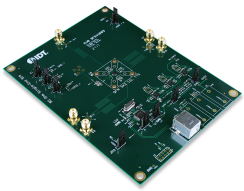
Evaluation Kit for 9FGV1005 Programmable PhiClock™ Generator
This is the evaluation board for the 9FGV1005 programmable PhiClockTM generator. It provides a convenient way of configuring and programming the blank parts for the 9FGV1005 device. With the onboard USB interface, the Renesas Timing CommanderTM Graphical User Interface (GUI) can communicate with... 阅读详情
Evaluation Kit for 9FGV1005 Programmable PhiClock™ Generator with Internal 50MHz Crystal
This is the evaluation board for the 9FGV1005Q5 programmable PhiClockTM generator with internal 50MHz crystal. It provides a convenient way of configuring and programming the blank parts for the 9FGV1005Q5 device. With the onboard USB interface, the Renesas Timing CommanderTM graphical user... 阅读详情
筛选
当前筛选条件
软件与工具
按类型筛选
按供应商筛选
样例程序
按应用筛选
按功能筛选
按编译器筛选
按 IDE 筛选
模拟模型
Partner Solutions
No Results Found.
确保所有关键词拼写正确。
尝试使用更少、不同或更宽泛的词语来改变搜索结果。
如果您使用了筛选器,请考虑取消选择某些筛选器选项以扩大搜索结果。
- 搜索我们丰富的知识库,帮助您解答常见问题
- 前往支持论坛,获取瑞萨电子技术专家和社群的帮助
软件与工具 (2)
No Results Found.
确保所有关键词拼写正确。
尝试使用更少、不同或更宽泛的词语来改变搜索结果。
如果您使用了筛选器,请考虑取消选择某些筛选器选项以扩大搜索结果。
- 搜索我们丰富的知识库,帮助您解答常见问题
- 前往支持论坛,获取瑞萨电子技术专家和社群的帮助
模拟模型 (1)
No Results Found.
确保所有关键词拼写正确。
尝试使用更少、不同或更宽泛的词语来改变搜索结果。
如果您使用了筛选器,请考虑取消选择某些筛选器选项以扩大搜索结果。
- 搜索我们丰富的知识库,帮助您解答常见问题
- 前往支持论坛,获取瑞萨电子技术专家和社群的帮助
Ron Wade, chief PCIe system architect explains the fundamental difference in reference clock jitter budgets between the first three generations of the specification and those of Gen4 and Gen5 which raise new challenges for designers.
This whiteboard video presents a brief overview comparing the evolution of PCI Express data rates through five generations versus that of the common clock jitter specifications.
Renesas's chief PCIe system architect explains how to derive separate reference clock jitter limits from the PCI Express Gen4 and Gen5 specifications.
The IDT PhiClock™ 9FGV100x PCIe Gen 4 clock generators combine space savings, high performance and low power in a single, easy-to-use solution. All PhiClock PCIe reference clock devices integrate crystal load capacitors and offer an optional integrated crystal to simplify designs and save board space. When configured with HCSL outputs for PCIe applications, PhiClock products integrate the output termination resistors, further reducing board space. Extremely small 3 x 3 mm and 4 x 4 mm packages complement the integration for maximum space savings. The programmable PhiClock clock generators combine outstanding PCIe Gen4 performance and outstanding Ethernet performance with phase jitter as low as 225fs rms at 156.25MHz (12k-20M). Extremely low power consumption (as low as 100 mW at 1.8V) allows placement closer to high-power components, which also reduces board space requirements.
A detailed overview of IDT's full-featured PCI Express (PCIe) clock and timing solutions. The presentation addresses PCIe Gen 1, Gen 2, Gen 3, and Gen 4 architectures and how IDT's industry-leading solutions provide all the functions, features, and performance required by the application.
Presented by Ron Wade, System Architect at IDT. For more information visit the PCIe clocks page.
This is the first video in our PCIe series. In this video, we define PCIe architectures, focusing on common and separate clock architectures. Watch the rest of the video series below where Ron will cover the impact of different timing architectures.
In this episode, Ron Wade from IDT (acquired by Renesas) explains PCIe common clocking and its impact on timing solutions. Learn about using a single clock source, fan-out buffers, and the considerations for spread spectrum and non-spread spectrum clocking in PCIe systems.
In this video, we explore PCIe with separate reference clocks and the effects of clock selection. Learn how separate reference clocks work and their impact on system performance and stability.
This video provides a high-level overview of Separate Reference Clock with Independent Spread (SRIS) architectures for PCI Express systems, additional performance requirements that this clocking architecture imposes on the reference clocks, and some system implications encountered trying to implement the architecture.
IDT (acquired by Renesas) engineer provides a brief tutorial describing the main differences between standard HCSL and low-power HCSL (LP-HCSL).
Presented by Ron Wade, PCI Express timing expert.
An overview of IDT's full-featured PCI Express (PCIe) clock generators addressing PCIe Gen 1, Gen 2, Gen 3, and Gen 4.
Presented by Ron Wade, System Architect at IDT.
An overview of PCI Express applications and how IDT's industry-leading portfolio of PCIe clock products addresses the requirements. The video briefly discusses PCIe riser cards, embedded SOC, and PCIe storage (NVME) examples.
Presented by Ron Wade, System Architect at IDT.
A brief overview of how data rates have changed from PCI Express (PCIe) Generation 1, Gen 2, Gen 3, Gen 4 and Gen 5.
Presented by Ron Wade, system architect at IDT.
A brief overview of how clock and timing specifications have changed from PCI Express (PCIe) Generation 1, Gen 2, Gen 3, Gen 4 and Gen 5.
Presented by Ron Wade, system architect at IDT (acquired by Renesas).
A brief overview of the PCI Express common clock (CC) jitter model, and the transfer functions as they relate to the timing PLLs. This model applies to PCI Express (PCIe) Gen 2, Gen 3, Gen 4 and Gen 5. The equations would be slightly different for other PCIe architectures, such as SRIS, SRnS, or data clocked.
Presented by Ron Wade, system architect at IDT (acquired by Renesas). For more information about Renesas's PCIe timing solutions, visit the PCI Express (PCIe) Clocks page.


