
| CAD 模型: | View CAD Model |
| Pkg. Type: | FCCSP |
| Pkg. Code: | BV0264AA |
| Lead Count (#): | 264 |
| Pkg. Dimensions (mm): | 8.7 x 14.4 x 0.9 |
| Pitch (mm): | 0.6 |
| Moisture Sensitivity Level (MSL) | 3 |
| Pb (Lead) Free | Yes |
| ECCN (US) | |
| HTS (US) |
| Pkg. Type | FCCSP |
| Lead Count (#) | 264 |
| Carrier Type | Tray |
| Moisture Sensitivity Level (MSL) | 3 |
| Qty. per Reel (#) | 0 |
| Qty. per Carrier (#) | 170 |
| Pb (Lead) Free | Yes |
| Pb Free Category | e8 SnAgCu |
| Temp. Range (°C) | 0 to 70°C |
| Application System | Server |
| Function | DDR5 Gen 2 MRDIMM MRCD |
| Length (mm) | 8.7 |
| MOQ | 170 |
| Pitch (mm) | 0.6 |
| Pkg. Dimensions (mm) | 8.7 x 14.4 x 0.9 |
| Product Type | Registering Clock Driver |
| Tape & Reel | No |
| Thickness (mm) | 0.9 |
| Width (mm) | 14.4 |
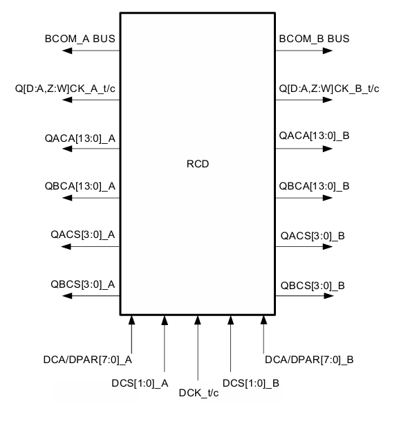
The RRG5012X-A00 is a second-generation Multiplexing Registering Clock Driver (MRCD) used on DDR5 MRDIMMs. Its primary function is to buffer the Command/Address (CA) bus, chip selects, and clock between the host controller and the DRAMs. It also creates a BCOM bus that controls the data buffers. The RRG5012X-A00 contains two separate channels with some common logic such as clocking, but which otherwise operate independently of each other. For each channel, the host interface is a 7-bit + parity/CRC CA bus with two chip-select inputs, running at single or double data rate and 1x or 2x the DRAM frequency.
Both Mux Mode and Rank Mode are supported. In Mux Mode, up to two ranks per each of two multiplexed pseudo-channels are supported, allowing simultaneous operation in the same direction. The RRG5012X-A00 demultiplexes the pseudo-channels and transmits each to a separate DRAM output interface. Rank Mode does not use pseudo-channels and operates as a four-rank LRDIMM.
Each DRAM interface is a 14-bit single data rate CA bus output with a chip-select. The RRG5012X-A00 also transcodes commands from the CA bus onto a per-channel BCOM bus for data buffer control. The RRG5012X-A00 has a common clock input and PLL, but produces eight separate clock pairs to the DRAM channels.
