特性
- Configurable OE pin function as OE, PD#, PPS, or DFC control function
- Configurable PLL bandwidth/minimizes jitter peaking
- PPS: Proactive Power Saving features save power during the end device power down mode
- PPB: Performance- Power Balancing feature allows minimum power consumption based on the required performance
- DFC: Dynamic Frequency Control feature allows up to 4 different frequencies to switch dynamically
- Features <65µA ultra-power-down
- Outputs: 1MHz to 125MHz
- Spread Spectrum clock support to lower system EMI
- I2C interface
- Supported by Renesas' Timing Commander™ software tool


描述
The 5L35021 is a VersaClock® programmable clock generator designed for low-power, consumer, and high-performance PCI Express applications. The 5L35021 device is a three-PLL architecture design, and each PLL is individually programmable and allows for up to five unique frequency outputs.
The 5L35021 has built-in unique features such as Proactive Power Saving (PPS), Performance-Power Balancing (PPB), Overshot Reduction Technology (ORT), and Extreme Low Power DCO. An internal OTP memory allows the user to store the configuration in the device without programming after power up, and then program the 5L35021 again through the I2C interface.
The device has programmable VCO and PLL source selection to allow the user to do power-performance optimization based on the application requirements. It also supports one single-ended output and two pairs of differential outputs that support LVCMOS and LPHCSL. A low-power 32.768kHz clock is supported with less than 2μA current consumption for the system RTC reference clock.
产品参数
| 属性 | 值 |
|---|---|
| App Jitter Compliance | PCIe Gen1, PCIe Gen2, PCIe Gen3 |
| Outputs (#) | 5 |
| Output Type | LVCMOS, LP-HCSL |
| Output Freq Range (MHz) | 0.032768 - 125 |
| Input Freq (MHz) | 1 - 160 |
| Inputs (#) | 1 |
| Input Type | Crystal, LVCMOS, LVPECL, LVDS, HCSL |
| Output Banks (#) | 3 |
| Core Voltage (V) | 1.8 |
| Output Voltage (V) | 1.8 |
| Feedback Input | No |
| Product Category | VersaClock 3S, Low Jitter Clocks (<700 fs RMS), General Purpose Clocks, Programmable Clocks |
| Selection Criteria | <700 fs RM |
封装选项
| Pkg. Type | Pkg. Dimensions (mm) | Lead Count (#) | Pitch (mm) |
|---|---|---|---|
| VFQFPN | 3.0 x 3.0 x 1.0 | 20 | 0.4 |
产品对比
| 5L35021 | 5P35021 | 5P35023 | 5L35023 | |
| Outputs (#) | 5 | 5 | 7 | 7 |
| Output Type | LP-HCSL, LVCMOS | LP-HCSL, LVCMOS, LVDS, LVPECL | LP-HCSL, LVCMOS, LVDS, LVPECL | LP-HCSL, LVCMOS |
| Core Voltage (V) | 1.8 | 3.3 | 3.3 | 1.8 |
| Output Voltage (V) | 1.8 | 1.8, 2.5, 3.3 | 1.8, 2.5, 3.3 | 1.8 |
| Pkg. Dimensions (mm) | 3.0 x 3.0 x 1.0 | 3.0 x 3.0 x 1.0 | 4.0 x 4.0 x 0.9 | 4.0 x 4.0 x 0.9 |
应用
- Embedded computing devices
- Consumer application crystal oscillator replacements
- SmartDevice, handheld, and consumer applications
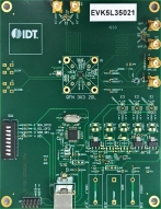
Renesas Boards & Kits
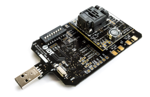
5L35021 VersaClock 3S Programmable Clock Development Kit
The DEV5L35021 programmable clock development kit is designed to support the 5L35021 VersaClock 3S device. It provides a convenient way of configuring and programming the blank parts for the 5L35021 device. With the on-board USB interface, the Renesas Timing CommanderTM graphical user interface... 阅读详情