特性
- Configurable OE pin function as OE, PD#, PPS, or DFC control function
- Configurable PLL bandwidth/minimizes jitter peaking
- PPS: Proactive Power Saving features save power during the end device power down mode
- PPB: Performance- Power Balancing feature allows minimum power consumption based on required performance
- DFC: Dynamic Frequency Control feature allows up to 4 different frequencies to switch dynamically
- Features < 65µA ultra-power-down
- Outputs: 1MHz to 125MHz
- Spread Spectrum clock support to lower system EMI
- I²C interface
- Supported by Renesas' Timing Commander™ software tool


描述
The 5L35023 is a VersaClock® programmable clock generator designed for low-power, consumer, and high-performance PCI Express applications. The 5L35023 device is a three-PLL architecture design, and each PLL is individually programmable and allows for up to five unique frequency outputs.
The 5L35023 has built-in unique features such as Proactive Power Saving (PPS), Performance-Power Balancing (PPB), Overshot Reduction Technology (ORT), and Extreme Low Power DCO. An internal OTP memory allows the user to store the configuration in the device without programming after power up, and then program the 5L35023 again through the I²C interface.
The device has programmable VCO and PLL source selection to allow the user to do power-performance optimization based on the application requirements. It also supports three single-ended outputs and two pairs of differential outputs that support LVCMOS and LPHCSL. A low-power 32.768kHz clock is supported with less than 2μA current consumption for the system RTC reference clock.
产品参数
| 属性 | 值 |
|---|---|
| App Jitter Compliance | PCIe Gen1, PCIe Gen2, PCIe Gen3 |
| Outputs (#) | 7 |
| Output Type | LVCMOS, LP-HCSL |
| Output Freq Range (MHz) | 0.032768 - 125 |
| Input Freq (MHz) | 1 - 160 |
| Inputs (#) | 1 |
| Input Type | Crystal, LVCMOS, LVPECL, LVDS, HCSL |
| Output Banks (#) | 5 |
| Core Voltage (V) | 1.8 |
| Output Voltage (V) | 1.8 |
| Product Category | VersaClock 3S, General Purpose Clocks, Programmable Clocks |
封装选项
| Pkg. Type | Pkg. Dimensions (mm) | Lead Count (#) | Pitch (mm) |
|---|---|---|---|
| VFQFPN | 4.0 x 4.0 x 0.9 | 24 | 0.5 |
产品对比
应用方框图
 | 自主移动机器人(AMR) 具备 AI 功能的 AMR 系统,集实时控制、可扩展电源和紧凑设计于一体。 |
 | 服务机器人 一款集成实时控制技术的 AI 驱动型服务机器人,可实现智能、安全、高效的导航。 |
 | AI 行车记录仪 采用 AI 技术的行车记录仪,具备高性能视觉处理、ADAS 和实时智能分析功能。 |
 | 基于 RZ/V2N 的 Raspberry Pi 单板计算机 高性能视觉 AI 系统,支持 4K 摄像头、高效的 AI 处理和紧凑的 SBC 设计。 |
 | 无线电子游戏桌 灵活的 Wi-Fi 6 系统提供 3000Mbps、4x4 MIMO、双频支持以及无缝集成功能。 |
 | 具有 AI 功能的可扩展人机界面 SMARC SoM 可扩展的 SoM,具有多核处理、高级图形和强大的连接性,适用于智能人机界面(HMI)。 |
其他应用
- Embedded computing devices
- Consumer application crystal oscillator replacements
- SmartDevice, handheld, and consumer applications
完成您的设计
寻找相关的产品,完善您的设计
Renesas Boards & Kits
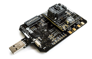
5L35023 VersaClock 3S Programmable Clock Development Kit
The DEV5L35023 programmable clock development kit is designed to support the 5L35023 VersaClock 3S device. It provides a convenient way of configuring and programming the blank parts for the 5L35023 device. With the on-board USB interface, the Renesas Timing CommanderTM graphical user interface... 阅读详情
Evaluation Board for 5L35023 VersaClock 3S
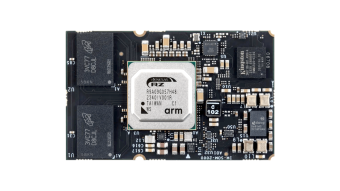
RZ/V2H 四核视觉 AI MPU 评测套件
RZ/V2H AI MPU 评测套件 (RTK0EF0168C04000BJ) 用于评测瑞萨电子 RZ/V2H 四核视觉 AI MPU。 该套件包括 CPU 板和扩展 (EXP) 板。 支持 RZ/V2H 标准软件包,能轻松实现低功耗 AI 推理和视频流等软件开发任务。 此外,这款评测套件还支持图像信号处理器 (ISP)、3D 图形引擎 (GE3D) 和可信安全 IP 等可选功能。
远程测试该板卡
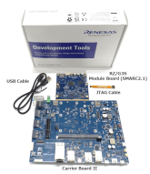
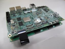
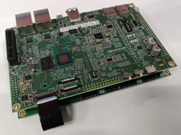
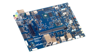
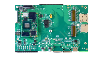
RZ/G3S 评估板套件
该评估板套件适用于评估 RZ/G3S。 RZ/G3S 评估板套件由模块板 (SOM) 和扩展板组成。 模块板符合 SMARC v2.1 标准。
- 目录
- RZ/G3S SMARC 模块板 (SMARC2.1)
- RZ SMARC 系列扩展板 II
- RZ SMARC 系列 JTAG 适配器电缆
- USB Type-A 转 USB Micro B 电缆,用于串行调试
- 配件:螺丝和垫片
*请自行准备以下内容:
- 65W USB Type-C 充电器
- USB PD 支持
- 输出:5V3A,9V3A,15V3A,20V3.25A
- USB Type-C 转 Type-C 电缆
- USB-C&USB-C 3.1 Gen2 USB-PD...
RZ/V2N 四核视觉 AI MPU 评测套件
RZ/V2N AI MPU 评测套件 (RTK0EF0186C03000BJ) 用于评测我们的 RZ/V2N 四核 视觉 AI MPU。 该套件包括一块 CPU 评测板、扩展 (EXP) 板和两块子板。 我们提供了 AI 软件开发包 (AI SDK) 作为该评测套件的软件开发环境。 它支持对低功耗 AI 推理、视频流和其他内置功能进行评测。 该套件还支持图像信号处理器 (ISP)、3D 图形引擎 (GE3D) 和可信安全 IP 等可选功能。
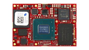
RZ/G3E MPU 评测板套件
RZ/G3E 评测板套件由模块板 (SOM) 和扩展板组成,是评测 RZ/G3E MPU 功能的理想之选。 模块板符合 SMARC v2.1 标准,是基于模块板进行产品开发的良好参考。
主要配件:
- RZ/G3E SMARC 模块板 (SMARC2.1)
- RZ SMARC 系列扩展板 II(与 RZ/G3S-EVKIT 通用)
- 各种适配器板、电缆、螺钉等
*请自行准备以下设备:
- 65W USB Type-C 充电器和 USB Type-C 至 Type-C 连接线
- USB PD 支持
- 输出:5V3A、9V3A、15V3A、20V3.25A
- 微型标清 UHI 级 10 8GB 或以上
*有关更多信息,请参阅... 阅读详情
Partner Boards & Kits
Banana PI BPI-AI2H System on Module (SoM)
Banana Pi BPI-AI2N System on Module (SoM) & BPI-AI2N Carrier
E1M-X V2N System on Module (SoM)
E1M-X V2N-M1
HummingBoard RZ/V2N AIOT
OSM Size M System on Module (SoM) for Industrial Applications
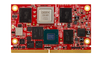
RZ/G3E DX-M1 System on Module (SoM)
RZ/G3E OSM-L
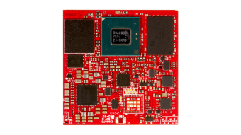
RZ/G3E System on Module (SoM)
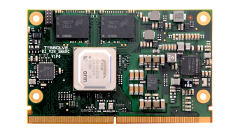
RZ/V2H SMARC Module
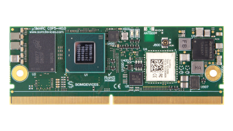
SOMDEVICES uSMARC RZ/V2N
TIA RZ/V2H
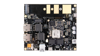
V2H 4X SBC
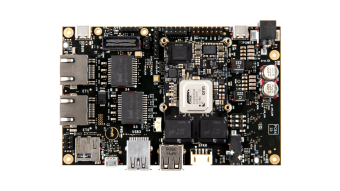
V2H Single Board Computer (SBC)