特性
- Configurable OE pin function as OE, PD#, PPS, or DFC control function
- Configurable PLL bandwidth/minimizes jitter peaking
- PPS: Proactive Power Saving features save power during the end device power down mode
- PPB: Performance Power Balancing feature allows minimum power consumption based on required performance
- DFC: Dynamic Frequency Control feature allows up to 4 different frequencies to switch dynamically
- Spread spectrum clock support to lower system EMI
- I2C interface
- Also supports crystal input
- Supported by the Timing Commander™ software tool
- Available in AEC-Q100 qualified, Grade 2 (-40 °C to +105 °C) version


描述
The 5P35023 is a VersaClock® programmable clock generator designed for low-power, consumer, and high-performance PCI Express applications. The 5P35023 device is a three-PLL architecture design, and each PLL is individually programmable and allows for up to five unique frequency outputs. The 5P35023 has built-in unique features such as Proactive Power Saving (PPS), Performance-Power Balancing (PPB), Overshot Reduction Technology (ORT), and Extreme Low Power DCO. An internal OTP memory allows the user to store the configuration in the device without programming after powering up, and then program the 5P35023 again through the I2C interface.
The device has programmable VCO and PLL source selection to allow the user to do power-performance optimization based on the application requirements. It also supports three single-ended outputs and two pairs of differential outputs that support LVCMOS, LVPECL, LVDS, and LPHCSL. A low-power 32.768kHz clock is supported with only less than 5μA current consumption for the system RTC reference clock.
产品参数
| 属性 | 值 |
|---|---|
| Diff. Outputs | 2 |
| App Jitter Compliance | PCIe Gen1, PCIe Gen2, PCIe Gen3 |
| Outputs (#) | 7 |
| Output Type | LVCMOS, LVPECL, LP-HCSL, LVDS |
| Output Freq Range (MHz) | 0.032768 - 500 |
| Input Freq (MHz) | 1 - 160 |
| Inputs (#) | 1 |
| Input Type | Crystal, LVCMOS, LVPECL, LVDS, LP-HCSL |
| Output Banks (#) | 5 |
| Core Voltage (V) | 3.3 |
| Output Voltage (V) | 1.8V, 2.5V, 3.3V |
| Product Category | VersaClock 3S, Automotive Timing, General Purpose Clocks, PCI Express Clocks, Programmable Clocks |
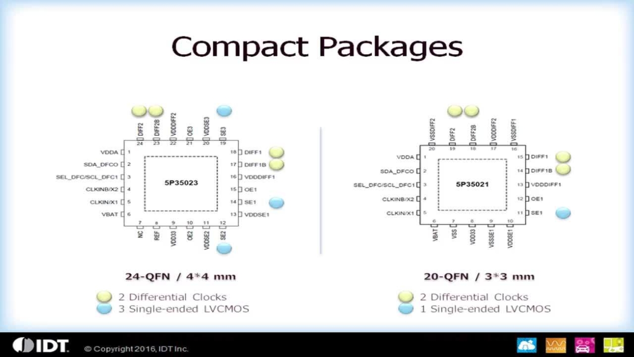
封装选项
| Pkg. Type | Pkg. Dimensions (mm) | Lead Count (#) | Pitch (mm) |
|---|---|---|---|
| VFQFPN | 4.0 x 4.0 x 0.9 | 24 | 0.5 |
产品对比
| 5P35023 | 5P35021 | 5L35021 | 5L35023 | |
| Outputs (#) | 7 | 5 | 5 | 7 |
| Output Type | LP-HCSL, LVCMOS, LVDS, LVPECL | LP-HCSL, LVCMOS, LVDS, LVPECL | LP-HCSL, LVCMOS | LP-HCSL, LVCMOS |
| Core Voltage (V) | 3.3 | 3.3 | 1.8 | 1.8 |
| Output Voltage (V) | 1.8, 2.5, 3.3 | 1.8, 2.5, 3.3 | 1.8 | 1.8 |
| Pkg. Dimensions (mm) | 4.0 x 4.0 x 0.9 | 3.0 x 3.0 x 1.0 | 3.0 x 3.0 x 1.0 | 4.0 x 4.0 x 0.9 |
应用方框图
 | 宠物摄像机器人 具有实时视频、音频和无线控制功能的移动宠物摄像机器人。 |
 | 高端中央温控器 中央温控系统集成了卫星式温控器,可实现智能气候调控与能效管理。 |
 | 具有 AI 功能的视频会议摄像头 配备双摄像头和波束成形拾音的 AI 驱动型 360° 视频会议系统。 |
 | 高端功能丰富的 HMI 平台 灵活的 HMI 平台,为显示分辨率、音频、扬声器等提供丰富的功能支持。 |
 | 单板计算机网关 带有 Arm Cortex-A55 和 Arm Cortex-M33 内核的 SBC 网关提供高效的处理、灵活性和连接性。 |
 | 电池供电摄像头,拥有人工智能物体检测和运动感应功能 电池供电人工智能摄像头,具有高效的运动检测、快速启动和低功耗物体分类功能。 |
 | 门禁系统,具有 NFC、摄像头和电容式触摸身份验证功能 门禁系统通过 NFC、Wi-Fi、PoE、本地存储和灵活的操作系统支持确保安全性。 |
 | 便携式 POS 终端 便携式移动 POS 机,支持安全、无线和多种支付方式,可在任何地方进行流畅的交易。 |
 | 视觉 AI 盒 作为集中控制枢纽,用于管理多路摄像头和 AI 模型。 |
 | 智能遥控即热式燃气热水器 无水箱燃气热水器采用远程控制、紧凑型双芯片 MCU 设计和精确的温度控制。 |
 | 未来 E/E 架构的车载电脑 下一代车载计算机系统,用于具有高计算能力的高级 E/E 架构。 |
 | 人工智能监控摄像机 具有 DRP-AI 功能的 AI 监控摄像机可通过 4K 成像和低功耗提高安全性。 |
 | 物联网通信网关中心 智能通信网关通过蓝牙 LE、NFC 和云连接将患者数据与医生同步。 |
 | 高级 HMI 和边缘 AI 应用的单板计算机 紧凑型 SBC 通过双核 MPU、DRP-AI、Wi-Fi、蓝牙 LE 和 NFC 连接支持 HMI 和边缘 AI。 |
 | 高性价比数字集群,配备四通道 AHL 和环视功能 数字集群通过集中信息并通过 AHL 和高效的 PMIC 降低成本来提高安全性。 |
完成您的设计
寻找相关的产品,完善您的设计
Renesas Boards & Kits
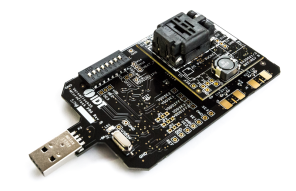
5P35023 and 5X35023 VersaClock 3S Programmable Clock Development Kit
The DEV5P35023 programmable clock development kit is designed to support the 5P35023 and 5X35023 VersaClock 3S devices. It provides a convenient way of configuring and programming the blank parts for the 5P35023 and 5X35023 devices. With the onboard USB interface, the Renesas Timing CommanderTM... 阅读详情
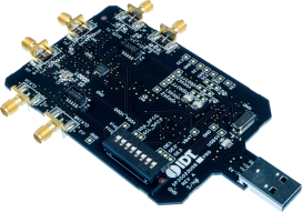
Programmer Board for VersaClock 3S - 5P3502x
The VersaClock® 3S-5P3502x programmer board is made to ease the programming of blank 5P35021 and 5P35023 devices. With the on-board USB interface, the Renesas Timing Commander™ graphical user interface (GUI) is used to communicate with the blank device in the socket for configuration and... 阅读详情
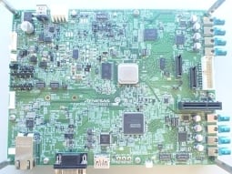
ADAS & Automated Driving Solution R-Car V3H Development Board/Condor-I
The combination of the R-Car, the PMIC, and the clock generators provides a high-efficiency and high-end ADAS solution that supports image input, image output, and high-speed input/output IF.
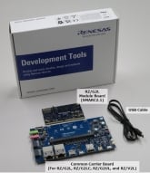
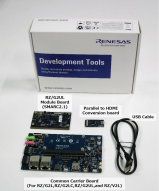
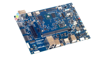
RZ/G2L MPU 评估板套件
该评估板套件适用于评估 RZ/G2L。 RZ/G2L 评估板套件由模块板(SOM)和扩展板组成。 模块板符合 SMARC v2.1 标准。
- 目录
- RZ/G2L 模块板(SMARC2.1)
- 公共载板(用于 RZ/G2L、RZ/G2LC、RZ/G2UL 和 RZ/V2L)
- USB 电缆(USB Type-A- Micro USB Type-B)
*请自行准备以下设备:
- 65W USB Type-C 充电器
- USB PD 接口
- 输出:5V3A、9V3A、15V3A、20V3.25A
- USB Type-C 转 Type-C 电缆
- 支持 USB-C 和 USB-C 3.1 Gen2 USB-PD 100W
- 微型标清... 阅读详情
远程测试该板卡
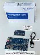
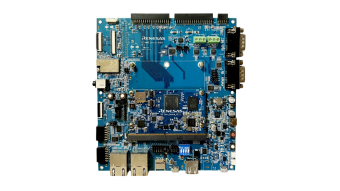
RZ/G2LC 评估板套件
该评估板套件适用于评估 RZ/G2LC。 RZ/G2LC 评估板套件由模块板 (SOM) 和扩展板组成。 SOM 符合 SMARC v2.1 标准。
- Contents
- RZ/G2LC Module Board (SMARC2.1)
- Common Carrier Board (For RZ/G2L, RZ/G2LC, RZ/G2UL and RZ/V2L)
- USB Cable (USB Type-A- Micro USB Type-B)
*Please prepare the following by yourself:
- 65W USB Type-C Charger
- USB PD
- Output:...
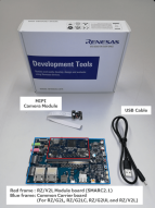
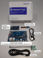
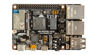
RZ/V2L 评估板套件
该评估板套件适用于评估 RZ/V2L。 RZ/V2L 评估板套件由模块板 (SOM) 和扩展板组成。 此外,产品附带 MIPI 摄像头模块 (MIPI CSI)。 扩展板通常适用于按照 SMARC v2.1 标准制备的 RZ/G2L,RZ/G2LC,RZ/G2UL,RZ/V2L模块 (SOM)。 基于这种适用性,在使用这些设备时,您可以体验到无缝且灵活的评估。
远程测试该板卡
RZ/G2UL MPU 评估板套件
该评估板套件适用于评估 RZ/G2UL。 RZ/G2UL 评测板套件由模块板(SOM)和扩展板组成。 模块板符合 SMARC v2.1 标准。
配件:
- RZ/G2UL 模块板(SMARC2.1)
- 公共载板(用于 RZ/G2L、RZ/G2LC、RZ/G2UL 和 RZ/V2L)
- USB 数据线(USB Type-A、Micro USB Type-B)
*请自行准备以下设备:
- 65W USB Type-C 充电器
- USB PD 接口
- 输出:5V3A,9V3A,15V3A,20V3.25A
- USB Type-C 转 Type-C 电缆
- USB-C 和 USB-C 3.1 Gen2 USB-PD 100W... 阅读详情
RZ/A3UL 评估板套件
此评估板套件特别适用于评估 RZ/A3UL。 RZ/A3UL 评估板套件由模块板 (SOM) 和扩展板组成。 SOM 符合 SMARC v2.1 标准。
有两种类型的评估板:QSPI版本和Octal SPI版本。
- QSPI版本:内存配置/QSPI串行闪存(Boot) + DDR4:RTK9763U02S01002BE
- Octal-SPI版本:内存配置/ Octa 闪存(Boot) + Octa RAM + DDR4:RTK9763U02S01003BE
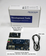
RZ/Five 评估板套件
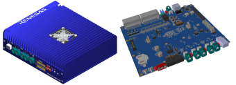
Vehicle Computer Generation 4
The VC4 is based on a complete Renesas chipset. The centerpiece is the R-Car S4 with 8x Cortex®A55 cores, 1x Cortex® R52 core 2x RH850 G4MH delivering up to 27K DMIPS application performance and up to 5.3K DMIPS lock step real-time performance. It incorporates an 8MB SRAM to execute code on the... 阅读详情
RZ/G3E MPU 评测板套件
RZ/G3E 评测板套件由模块板 (SOM) 和扩展板组成,是评测 RZ/G3E MPU 功能的理想之选。 模块板符合 SMARC v2.1 标准,是基于模块板进行产品开发的良好参考。
主要配件:
- RZ/G3E SMARC 模块板 (SMARC2.1)
- RZ SMARC 系列扩展板 II(与 RZ/G3S-EVKIT 通用)
- 各种适配器板、电缆、螺钉等
*请自行准备以下设备:
- 65W USB Type-C 充电器和 USB Type-C 至 Type-C 连接线
- USB PD 支持
- 输出:5V3A、9V3A、15V3A、20V3.25A
- 微型标清 UHI 级 10 8GB 或以上
*有关更多信息,请参阅... 阅读详情
Partner Boards & Kits
OSM-L System on Module (SoM) Powered by RZ/G2L
REGULUS RZ/V2L & RZ/G2L SMARC System on Module (SoM)
RZ/G2L SMARC 2.1 Compliant System on Module (SoM)
RZ/G2L SMARC System on Module (SoM)
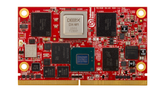
RZ/G3E DX-M1 System on Module (SoM)
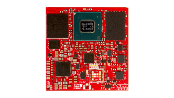
RZ/G3E OSM-L
RZ/G3E System on Module (SoM)
RZ/V2L SMARC 2.1 Compliant System on Module (SoM)
TRIA SM2S-G2L
TRIA SM2S-V2L
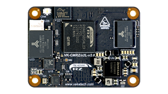
VK-CM-RZ/V2L
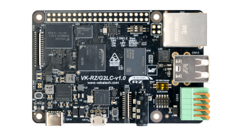
VK-RZ/G2LC
VK-RZ/V2L
RZ/V2L PerCV.AI Reference Design
Our RZ/V2L SoM offers a versatile platform packed with features and connectivity options like wireless, USB, and CAN, simplifying the integration of system components. Paired with the RZ/V2L SoM MXT AI board, we empower developers to jumpstart hardware and software development with robust tools... 阅读详情
远程测试该板卡
知识库
-
RZ/Five: RZ/Five的评估板使用哪种时脈发生器?
使用VersaClock3S的5P35023B-629NLGI。我们提供了集成在评估板中的EXTAL和音频时钟以及用于各以太网PHY和音频DAC的时钟。 https://www.renesas.com/products/ ...
2022年9月21日 -
RZ/G2L, LC: 时钟
使用VersaClock3S的5P35023B-629NLGI。我们提供EXTAL和音频时钟,并为评估板上搭载的各以太网PHY和音频DAC分别提供时钟。
2021年10月27日


