
特性
- 通用兼容的引脚排列和命令集
- 标准块架构
- 支持四路 I/O、QPI 和 XiP 操作
- 双倍传输速率(DTR)操作频率最高 84MHz
- SPI 时钟频率最高 133MHz
- XiP 连续读取、包装和突发模式

AT25xLx NOR 闪存框图
描述
AT25QF0641C 是一款 64Mbit 串行外设接口(SPI)闪存器件,专为各种大批量生产的工业、消费类及互联设备而设计。 该器件可用于存储程序代码,这些代码可在系统启动期间从闪存复制到嵌入式或外部 RAM 中。 此外,该器件还支持通过就地执行(XiP)操作直接从闪存执行代码。
产品参数
| 属性 | 值 |
|---|---|
| Memory Class | Standard Flash |
| Memory Density | 64 |
| Operating Voltage Range (V) | 2.7 - 3.6 |
| Speed | 133 MHz |
| Interface | Quad SPI, QPI |
| Temp. Range (°C) | -40 to +85°C |
| Deep Power Down (µA) | 0.7 |
| Read Current (mA) | 5 |
| Key Benefit | Standard features |
产品对比
 | | |
| AT25QF0641C | AT25SF0641C | |
| Operating Voltage Range | 2.7 - 3.6 | 2.7 - 3.6 |
| Interface | QPI, Quad SPI | Dual SPI, QPI, Quad SPI, Single SPI |
| Read Current (mA) | 5 | 5 |
应用方框图
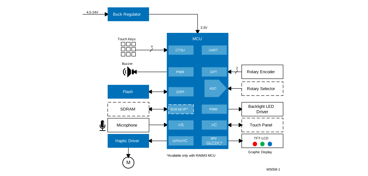 | 可扩展的中端图形 HMI 平台 可扩展的中端图形 HMI 设计将显示、触控和语音交互结合在一起,适用于各种集成式和互联式架构版本。 |
完成您的设计
寻找相关的产品,完善您的设计
| 器件号 | 状态 | 样品 | 供应期限 | 库存 | 封装 | 预算价格(美元) | Carrier Type | Moisture Sensitivity Level (MSL) | Assembly Location |
|---|---|---|---|---|---|---|---|---|---|
| AT25QF0641C-MUB-T | Active | Available | 2036 Aug | 缺货 | 5x6 DFN | 1ku | $0.923 | Tape & Reel | 3 | CHINA |
| AT25QF0641C-SUB-T | Active | Available | 2036 Aug | 缺货 | SOICW | 1ku | $0.832 | Tape & Reel | 3 | CHINA |
| AT25QF0641C-MBUB-T | Preview | N/A | 2036 Aug | 缺货 | 3x4 DFN | 1ku | $0.923 | Tape & Reel | 3 | CHINA |
| AT25QF0641C-MCUB-T | Preview | N/A | 2036 Aug | 缺货 | 4x4 DFN | 1ku | $0.935 | Tape & Reel | 3 | CHINA |
完成您的设计
寻找相关的产品,完善您的设计
加载中
- 数据手册英语PDF 4.15 MB R10DS0425EU0100 Rev.1.00 2026年8月07日The AT25SF0641C/AT25QF0641C is a 64Mbit SPI Serial NOR Flash memory operating from 2.7V to 3.6V. This datasheet describes its features, functions, command set, performance characteristics, package pinout, package specifications, and ordering information to support application design.
- 应用说明英语PDF 884 KB R10AN0038EU0100 Rev.1.00 2026年3月10日This application note discusses endurance and data retention in NOR Flash memory products. It describes the structure and operation of the NOR Flash transistor, the mechanisms of NOR Flash device failure and oxide degradation which limit endurance and data retention. It explains JEDEC-based test procedures for certifying endurance and data retention specifications and ways to mitigate limitations. The first part of this document and the appendix provide background for understanding the issue. The later sections describe practical scenarios of interest to most customers.
- 应用说明英语PDF 695 KB AN503 2025年9月05日Explores thermal resistance in integrated circuits (ICs) and details its role in managing heat from power consumption to ensure reliable operation. Proper thermal management enhances IC performance and longevity. Thermal resistance, measured in °C/W, quantifies heat flow resistance from the silicon die to the environment or PCB, with key types including junction-to-case (θJC), case-to-ambient (θCA), junction-to-ambient (θJA), and junction-to-board (θJB).
- 应用说明英语PDF 2.62 MB AN500 2024年2月13日AI 生成的摘要: NOR Flash memory requires an erase operation before programming, which occurs in three phases: Pre-Program, Erase, and Recovery. The erase process affects entire blocks simultaneously, not byte-by-byte. Memory cells use floating gate MOSFETs to store data, organized into arrays of rows (Word-Lines) and columns (Bit-Lines). Physical Blocks contain multiple Logical Blocks and share common p-wells and Bit-Lines, impacting operation. Smaller Logical Blocks enable improved erase performance through parallelization. Understanding these processes and potential interruptions is crucial for designing reliable systems.
- 应用说明英语PDF 710 KB AN502 2024年1月24日AI 生成的摘要: Renesas NOR flash devices require decoupling capacitors close to VCC and GND pins to stabilize voltage, typically 1 μF with an optional 100 nF capacitor. Pull-up resistors are recommended on CS#, WP#/IO2, and HOLD#/IO3 pins to ensure proper signal states and facilitate debugging. Signal routing should minimize trace length and maintain a solid ground plane for high-speed signals. Power supply must rise monotonically during power-up. Basic system bring-up involves verifying installation, voltage levels, and SPI communication using manufacturer/device ID commands. Software drivers depend on host MCU architecture; Renesas offers example drivers and support. Correct erase/program sequences include write-enable, erase/program commands, and status checks. Tools for programming include flash loader plug-ins and debug probes. Switching from single to quad-SPI involves setting the quad-enable bit, changing pin functions. Dummy cycles introduce necessary wait times during read commands to accommodate latency.
- 指南英语PDF 790 KB PBFLASH03102022 2023年6月16日
- 其他英语PDF 1 MB R10DS0315EU0000 Rev.0.00 2022年6月28日
- 应用说明英语PDF 794 KB 2022年5月12日AI 生成的摘要: Renesas NOR flash devices implement multiple protection methods to safeguard memory arrays, status registers, flash states, and resets from accidental or intentional modifications. Protection types include hardware-based write protection via the WP pin and software-based protection through commands controlling status registers and memory blocks. Memory array protection schemes include individual block protection, allowing sector-level lock/unlock, and memory edge protection, which protects contiguous regions aligned to memory edges. Status register protection indirectly secures memory by blocking changes to protection states. Detailed command sets and register bits configure these protections, ensuring robust flash memory integrity.
- 应用说明英语PDF 663 KB 2021年10月18日AI 生成的摘要: Proper power-up and power-down sequencing is critical for NOR Flash memory operation to ensure reliable system performance. The power supply voltage must ramp up monotonically without dips, reaching the minimum operational voltage within specified timing to avoid corrupted initialization. Reset methods, including hardware and JEDEC resets, help ensure the device starts from a known state. Brown-out conditions and power cycling require careful handling to prevent data corruption and ensure stable operation. The document covers power sequencing, reset types, brown-out recovery, power-down, and power-saving modes, providing essential guidelines for system engineers and application developers.
- 应用说明英语PDF 313 KB 2020年7月17日AI 生成的摘要: PCB design for Adesto memory devices requires careful placement of decoupling capacitors close to VCC and GND pins to minimize voltage fluctuations caused by parasitic inductance and capacitance in PCB traces. Proper capacitor selection and placement reduce signal integrity issues, EMI, and noise. Design guidelines vary by package type (SOIC, UDFN, WLCSP, BGA) and PCB layer count. Signal routing rules ensure reliable data and control signals. Special cases include parallel devices, reset signal handling, and test point integration. The document provides detailed layout recommendations for each package type to optimize device performance and reliability.
- 产品变更通告英语PDF 528 KB 2020年6月26日
- 数据手册英语PDF 4.15 MB R10DS0425EU0100 Rev.1.00 2026年8月07日The AT25SF0641C/AT25QF0641C is a 64Mbit SPI Serial NOR Flash memory operating from 2.7V to 3.6V. This datasheet describes its features, functions, command set, performance characteristics, package pinout, package specifications, and ordering information to support application design.
推荐文档 (1)
- 数据手册英语PDF 4.15 MB R10DS0425EU0100 Rev.1.00 2026年8月07日The AT25SF0641C/AT25QF0641C is a 64Mbit SPI Serial NOR Flash memory operating from 2.7V to 3.6V. This datasheet describes its features, functions, command set, performance characteristics, package pinout, package specifications, and ordering information to support application design.
数据手册 (1)
- 指南英语PDF 790 KB PBFLASH03102022 2023年6月16日
手册和指南 (1)
- 应用说明英语PDF 884 KB R10AN0038EU0100 Rev.1.00 2026年3月10日This application note discusses endurance and data retention in NOR Flash memory products. It describes the structure and operation of the NOR Flash transistor, the mechanisms of NOR Flash device failure and oxide degradation which limit endurance and data retention. It explains JEDEC-based test procedures for certifying endurance and data retention specifications and ways to mitigate limitations. The first part of this document and the appendix provide background for understanding the issue. The later sections describe practical scenarios of interest to most customers.
- 应用说明英语PDF 695 KB AN503 2025年9月05日Explores thermal resistance in integrated circuits (ICs) and details its role in managing heat from power consumption to ensure reliable operation. Proper thermal management enhances IC performance and longevity. Thermal resistance, measured in °C/W, quantifies heat flow resistance from the silicon die to the environment or PCB, with key types including junction-to-case (θJC), case-to-ambient (θCA), junction-to-ambient (θJA), and junction-to-board (θJB).
- 应用说明英语PDF 2.62 MB AN500 2024年2月13日AI 生成的摘要: NOR Flash memory requires an erase operation before programming, which occurs in three phases: Pre-Program, Erase, and Recovery. The erase process affects entire blocks simultaneously, not byte-by-byte. Memory cells use floating gate MOSFETs to store data, organized into arrays of rows (Word-Lines) and columns (Bit-Lines). Physical Blocks contain multiple Logical Blocks and share common p-wells and Bit-Lines, impacting operation. Smaller Logical Blocks enable improved erase performance through parallelization. Understanding these processes and potential interruptions is crucial for designing reliable systems.
- 应用说明英语PDF 710 KB AN502 2024年1月24日AI 生成的摘要: Renesas NOR flash devices require decoupling capacitors close to VCC and GND pins to stabilize voltage, typically 1 μF with an optional 100 nF capacitor. Pull-up resistors are recommended on CS#, WP#/IO2, and HOLD#/IO3 pins to ensure proper signal states and facilitate debugging. Signal routing should minimize trace length and maintain a solid ground plane for high-speed signals. Power supply must rise monotonically during power-up. Basic system bring-up involves verifying installation, voltage levels, and SPI communication using manufacturer/device ID commands. Software drivers depend on host MCU architecture; Renesas offers example drivers and support. Correct erase/program sequences include write-enable, erase/program commands, and status checks. Tools for programming include flash loader plug-ins and debug probes. Switching from single to quad-SPI involves setting the quad-enable bit, changing pin functions. Dummy cycles introduce necessary wait times during read commands to accommodate latency.
应用说明和白皮书 (8)
- 产品变更通告英语PDF 528 KB 2020年6月26日
产品通告(产品变更、EOL 等) (2)
No Results Found.
检查拼写
确保所有关键词拼写正确。
确保所有关键词拼写正确。
调整关键词
尝试使用更少、不同或更宽泛的词语来改变搜索结果。
尝试使用更少、不同或更宽泛的词语来改变搜索结果。
查看筛选器
如果您使用了筛选器,请考虑取消选择某些筛选器选项以扩大搜索结果。
如果您使用了筛选器,请考虑取消选择某些筛选器选项以扩大搜索结果。
需要帮助?
- 搜索我们丰富的知识库,帮助您解答常见问题
- 前往支持论坛,获取瑞萨电子技术专家和社群的帮助
No Results Found.
检查拼写
确保所有关键词拼写正确。
确保所有关键词拼写正确。
调整关键词
尝试使用更少、不同或更宽泛的词语来改变搜索结果。
尝试使用更少、不同或更宽泛的词语来改变搜索结果。
查看筛选器
如果您使用了筛选器,请考虑取消选择某些筛选器选项以扩大搜索结果。
如果您使用了筛选器,请考虑取消选择某些筛选器选项以扩大搜索结果。
需要帮助?
- 搜索我们丰富的知识库,帮助您解答常见问题
- 前往支持论坛,获取瑞萨电子技术专家和社群的帮助
No Results Found.
检查拼写
确保所有关键词拼写正确。
确保所有关键词拼写正确。
调整关键词
尝试使用更少、不同或更宽泛的词语来改变搜索结果。
尝试使用更少、不同或更宽泛的词语来改变搜索结果。
查看筛选器
如果您使用了筛选器,请考虑取消选择某些筛选器选项以扩大搜索结果。
如果您使用了筛选器,请考虑取消选择某些筛选器选项以扩大搜索结果。
需要帮助?
- 搜索我们丰富的知识库,帮助您解答常见问题
- 前往支持论坛,获取瑞萨电子技术专家和社群的帮助
No Results Found.
检查拼写
确保所有关键词拼写正确。
确保所有关键词拼写正确。
调整关键词
尝试使用更少、不同或更宽泛的词语来改变搜索结果。
尝试使用更少、不同或更宽泛的词语来改变搜索结果。
查看筛选器
如果您使用了筛选器,请考虑取消选择某些筛选器选项以扩大搜索结果。
如果您使用了筛选器,请考虑取消选择某些筛选器选项以扩大搜索结果。
需要帮助?
- 搜索我们丰富的知识库,帮助您解答常见问题
- 前往支持论坛,获取瑞萨电子技术专家和社群的帮助
No Results Found.
检查拼写
确保所有关键词拼写正确。
确保所有关键词拼写正确。
调整关键词
尝试使用更少、不同或更宽泛的词语来改变搜索结果。
尝试使用更少、不同或更宽泛的词语来改变搜索结果。
查看筛选器
如果您使用了筛选器,请考虑取消选择某些筛选器选项以扩大搜索结果。
如果您使用了筛选器,请考虑取消选择某些筛选器选项以扩大搜索结果。
需要帮助?
- 搜索我们丰富的知识库,帮助您解答常见问题
- 前往支持论坛,获取瑞萨电子技术专家和社群的帮助
No Results Found.
检查拼写
确保所有关键词拼写正确。
确保所有关键词拼写正确。
调整关键词
尝试使用更少、不同或更宽泛的词语来改变搜索结果。
尝试使用更少、不同或更宽泛的词语来改变搜索结果。
查看筛选器
如果您使用了筛选器,请考虑取消选择某些筛选器选项以扩大搜索结果。
如果您使用了筛选器,请考虑取消选择某些筛选器选项以扩大搜索结果。
需要帮助?
- 搜索我们丰富的知识库,帮助您解答常见问题
- 前往支持论坛,获取瑞萨电子技术专家和社群的帮助
No Results Found.
检查拼写
确保所有关键词拼写正确。
确保所有关键词拼写正确。
调整关键词
尝试使用更少、不同或更宽泛的词语来改变搜索结果。
尝试使用更少、不同或更宽泛的词语来改变搜索结果。
查看筛选器
如果您使用了筛选器,请考虑取消选择某些筛选器选项以扩大搜索结果。
如果您使用了筛选器,请考虑取消选择某些筛选器选项以扩大搜索结果。
需要帮助?
- 搜索我们丰富的知识库,帮助您解答常见问题
- 前往支持论坛,获取瑞萨电子技术专家和社群的帮助
- 其他英语PDF 1 MB R10DS0315EU0000 Rev.0.00 2022年6月28日
其他 (2)
No Results Found.
检查拼写
确保所有关键词拼写正确。
确保所有关键词拼写正确。
调整关键词
尝试使用更少、不同或更宽泛的词语来改变搜索结果。
尝试使用更少、不同或更宽泛的词语来改变搜索结果。
查看筛选器
如果您使用了筛选器,请考虑取消选择某些筛选器选项以扩大搜索结果。
如果您使用了筛选器,请考虑取消选择某些筛选器选项以扩大搜索结果。
需要帮助?
- 搜索我们丰富的知识库,帮助您解答常见问题
- 前往支持论坛,获取瑞萨电子技术专家和社群的帮助
加载中
筛选
当前筛选条件
软件与工具
按类型筛选
样例程序
按应用筛选
按功能筛选
按编译器筛选
按 IDE 筛选
模拟模型
合作伙伴解决方案
- 开发工具µISP 是一款紧凑型、独立且通用的解决方案,基于 Algocraft 的 WriteNow! 技术构建,专为生产环境设计。 技术,是一款支持 PMBus 的 DC/DC 单通道降压电源。 该产品是众多器件和设备的标配工具,支持多种编程协议(JTAG、SPI、UART、DAP、SWD、I2C、BDM、自定义协议等)。提供方: Algocraft Srl
- 开发工具WriteNow! 系统内编程器系列是编程行业的一项突破性产品。 该系列编程器支持来自不同制造商的大量器件(微控制器、存储器、CPLD 和其他可编程器件),且体积小巧,便于与 ATE/夹具集成。 产品既可独立工作,也可连接主机 PC(内置 RS-232、LAN 和 USB 连接功能),并配有易于使用的软件实用程序。提供方: Algocraft Srl
No Results Found.
检查拼写
确保所有关键词拼写正确。
确保所有关键词拼写正确。
调整关键词
尝试使用更少、不同或更宽泛的词语来改变搜索结果。
尝试使用更少、不同或更宽泛的词语来改变搜索结果。
查看筛选器
如果您使用了筛选器,请考虑取消选择某些筛选器选项以扩大搜索结果。
如果您使用了筛选器,请考虑取消选择某些筛选器选项以扩大搜索结果。
需要帮助?
- 搜索我们丰富的知识库,帮助您解答常见问题
- 前往支持论坛,获取瑞萨电子技术专家和社群的帮助
No Results Found.
检查拼写
确保所有关键词拼写正确。
确保所有关键词拼写正确。
调整关键词
尝试使用更少、不同或更宽泛的词语来改变搜索结果。
尝试使用更少、不同或更宽泛的词语来改变搜索结果。
查看筛选器
如果您使用了筛选器,请考虑取消选择某些筛选器选项以扩大搜索结果。
如果您使用了筛选器,请考虑取消选择某些筛选器选项以扩大搜索结果。
需要帮助?
- 搜索我们丰富的知识库,帮助您解答常见问题
- 前往支持论坛,获取瑞萨电子技术专家和社群的帮助
No Results Found.
检查拼写
确保所有关键词拼写正确。
确保所有关键词拼写正确。
调整关键词
尝试使用更少、不同或更宽泛的词语来改变搜索结果。
尝试使用更少、不同或更宽泛的词语来改变搜索结果。
查看筛选器
如果您使用了筛选器,请考虑取消选择某些筛选器选项以扩大搜索结果。
如果您使用了筛选器,请考虑取消选择某些筛选器选项以扩大搜索结果。
需要帮助?
- 搜索我们丰富的知识库,帮助您解答常见问题
- 前往支持论坛,获取瑞萨电子技术专家和社群的帮助
No Results Found.
检查拼写
确保所有关键词拼写正确。
确保所有关键词拼写正确。
调整关键词
尝试使用更少、不同或更宽泛的词语来改变搜索结果。
尝试使用更少、不同或更宽泛的词语来改变搜索结果。
查看筛选器
如果您使用了筛选器,请考虑取消选择某些筛选器选项以扩大搜索结果。
如果您使用了筛选器,请考虑取消选择某些筛选器选项以扩大搜索结果。
需要帮助?
- 搜索我们丰富的知识库,帮助您解答常见问题
- 前往支持论坛,获取瑞萨电子技术专家和社群的帮助
- 开发工具µISP 是一款紧凑型、独立且通用的解决方案,基于 Algocraft 的 WriteNow! 技术构建,专为生产环境设计。 技术,是一款支持 PMBus 的 DC/DC 单通道降压电源。 该产品是众多器件和设备的标配工具,支持多种编程协议(JTAG、SPI、UART、DAP、SWD、I2C、BDM、自定义协议等)。提供方: Algocraft Srl
- 开发工具WriteNow! 系统内编程器系列是编程行业的一项突破性产品。 该系列编程器支持来自不同制造商的大量器件(微控制器、存储器、CPLD 和其他可编程器件),且体积小巧,便于与 ATE/夹具集成。 产品既可独立工作,也可连接主机 PC(内置 RS-232、LAN 和 USB 连接功能),并配有易于使用的软件实用程序。提供方: Algocraft Srl


