特性
- Accepts input voltages above or below regulated output voltage
- Automatic bypass mode functionality
- Automatic and seamless transitions between buck and boost modes
- Input voltage range: 1.8V to 5.5V
- Selectable forced bypass power-saving mode
- Adaptive multilevel current limit scheme to optimize efficiency at low and high currents
- Output current: up to 800mA (VIN = 2.5V, VOUT = 3.3V)
- High efficiency: up to 98%
- 41μA quiescent current maximizes light-load efficiency
- Fully protected for over-temperature and undervoltage
- Small packages
- ISL9120 - 1.41mm x 1.41mm WLCSP
- ISL9120IR - 3mm x 3mm 12 Ld TQFN


描述
The ISL9120 and ISL9120IR are highly integrated buck-boost switching regulators that accept input voltages either above or below the regulated output voltage. The regulator automatically transitions between buck and boost modes without significant output disturbance. They also have automatic bypass functionality. When the input voltage is generally within 1% to 2% of the output voltage, there will be a direct bypass connection between the VIN and VOUT pins.
In addition to the automatic bypass functionality, the ISL9120 and ISL9120IR also have forced bypass functionality with the use of the BYP pin. The device is capable of delivering up to 800mA of output current (VIN = 2.5V, VOUT = 3.3V) and provides excellent efficiency due to its adaptive current limit Pulse Frequency Modulation (PFM) control architecture.
The ISL9120 and ISL9120IR are designed for stand-alone applications and support a 3.3V fixed output voltage or variable output voltages with an external resistor divider. The forced bypass power saving mode can be chosen if voltage regulation is not required. The device consumes less than 3.5µA of current over the operating temperature range in forced bypass mode.
The ISL9120 and ISL9120IR require only a single inductor and very few external components. Power supply solution size is minimized by the ISL9120 1.41mm x 1.41mm WLCSP package and the ISL9120IR 3mm x 3mm 12 Ld TQFN package.
产品参数
| 属性 | 值 |
|---|---|
| Topology [Rail 1] | Buck-Boost |
| Outputs (#) | 1 |
| Input Voltage (Min) [Rail 1] (V) | 1.8 |
| Input Voltage (Max) [Rail 1] (V) | 5.5 - 5.5 |
| Output Voltage (Min) [Rail 1] (V) | 1 |
| Output Voltage (Max) [Rail 1] (V) | 5.2 |
| Output Current (Max) [Rail 1] (A) | 0.8 |
| IQ [Rail 1] (µA) | 41 |
| Control Type | Hysteretic Mode |
| POR | Yes |
| SYNCH Capability | No |
| Peak Efficiency (%) | 98 |
| Qualification Level | Standard |
应用方框图
 | 健康监测手环 一款可穿戴的健康手环,它使用压电传感器读取用户的心率和呼吸。 |
 | 用于健康监测的可穿戴智能联网戒指 智能戒指将健康追踪与 NFC 充电和支付以及低功耗 LE 蓝牙功能相结合,可发挥高效性能。 |
| 太阳能定位跟踪器 太阳能定位跟踪器提供模块化设计、多功能连接和光伏能量收集。 | |
 | 自动抄表器(AMR)改装模块 AMR 改装模块提供了经济高效的计量方案、灵活的 MCU 设计以及更长的电池使用寿命。 |
 | 带无线控制的 PC 水冷系统 先进的 PC 水冷器,具有无线控制、散热高效和配置灵活等特点。 |
其他应用
- Smartphones and tablets
- Portable consumer and wearable devices
完成您的设计
寻找相关的产品,完善您的设计
Renesas Boards & Kits
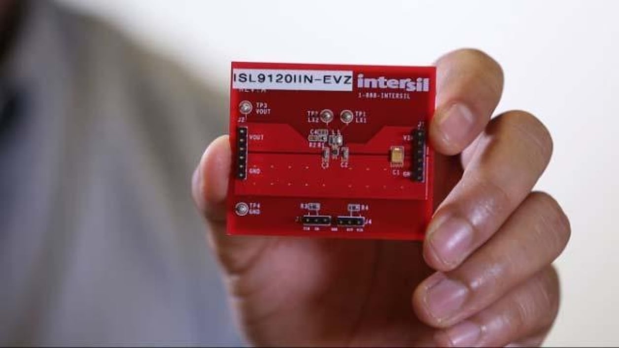
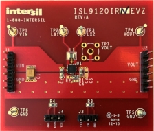
Compact High-Efficiency Low Power Buck-Boost Regulator Evaluation Board
Compact High-Efficiency Low Power Buck-Boost Regulator Evaluation Board
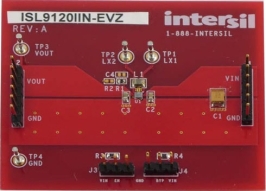
The ISL9120IIN-EVZ platform allows for quick evaluation of the high-performance features of the ISL9120 buck-boost regulator. The ISL9120IIN-EVZ evaluates the ISL9120IINZ featuring fixed 3.3V output.
The ISL9120 is a highly integrated buck-boost switching regulator for systems using new battery... 阅读详情
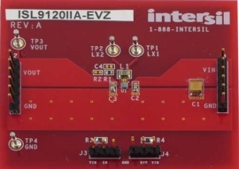
Compact High-Efficiency Low Power Buck-Boost Regulator Evaluation Board
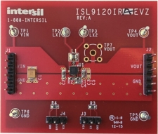
The ISL9120IRA-EVZ platform allows for quick evaluation of the high-performance features of the ISL9120IR buck-boost regulator. The ISL9120IRA-EVZ evaluates the ISL9120IRAZ featuring resistor programmable output voltage.
The ISL9120IR is a highly integrated buck-boost switching regulator for... 阅读详情
Compact High-Efficiency Low Power Buck-Boost Regulator Evaluation Board
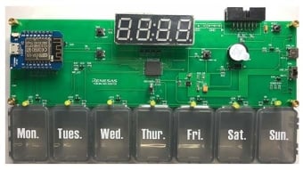
智能药盒参考设计
智能药盒专为确保患者按时用药而设计。 它使用专用的智能手机 APP,用户可以通过设置手机显示提醒管理其个人的用药物状态,并进行更多的操作。
该参考设计采用嵌入式 RL78/G13 MCU,通过 UART 与 Wi-Fi 模块进行通信。 通过 MQTT,使用瑞萨 IoT Sandbox 可校准实时时钟(RTC)计数值,设置或清除报警时间。 报警时间数据存储于数据闪存中。 ISL9120 高效降压-升压稳压器可以进一步提高功率控制的效率。
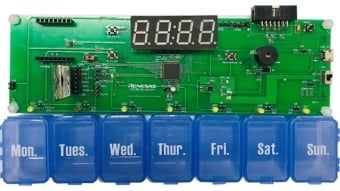
带低功耗蓝牙的智能药盒参考设计
智能药盒专为确保患者按时用药而设计。 它使用专用的智能手机 APP,用户可以通过设置手机显示提醒管理其个人的用药物状态,并进行更多的操作。
该参考设计采用嵌入式 RL78/G13 MCU,通过 UART 与 RL78/G1D 蓝牙 ® 低功耗(LE)模块进行通信。 ISL9120 高效降压-升压稳压器可以进一步提高功率控制的效率。
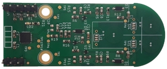
自动抄表器(AMR)改造模块参考设计
随着水表、热表和燃气表对自动抄表(AMR)功能的要求越来越高,许多公用事业公司决定为已部署的机械表使用 MID 认证的“即插即用”改造模块,作为在使用寿命到期之前完全更换为纯电子表的可行选项。 为了满足当前的市场需求,该设计采用了 16 位 RL78 MCU 内核技术,可以轻松地将传感器板连接到带有金属化分度轮的任何类型的机械水表上,并使用它来检测 RPM 和旋转方向。


