特性
- 逻辑和混合信号电路
- 高度灵活的宏单元
- 回读保护(Read Lock)
- 1.8V (±5%) 至 5V (±10%) 电源
- 工作温度范围:-40°C 至 85°C
- 符合 RoHS 标准/无卤素
- 宏单元总览
- 8 位逐次逼近寄存器模数转换器 (SAR ADC)
- ADC 3 位可编程增益放大器 (PGA)
- 2 个数模转换器 (DAC)
- 6 个模拟比较器 (ACMP)
- 两个电压基准 (Vref)
- 25 个组合查找表 (LUT)
- 8 个 2 位 LUT
- 16 个 3 位 LUT
- 1 个 4 位 LUT
- 1 个组合功能宏单元
- 模式发生器或 4 位 LUT
- 3 个数字比较器/脉宽调制器 (DCMP/PWM),具有可选的死区
- 10 个计数器/延迟 (CNT/DLY)
- 2 个 14 位延迟/计数器
- 1 个 14 位延迟/计数器(唤醒睡眠控制)
- 1 个 14 位延迟/计数器/有限状态机
- 5 个 8 位延迟/计数器
- 1 个 8 位延迟/计数器/有限状态机
- 12 个 D 触发器/锁存器
- 2 个管道延迟 – 16 级/2 路输出
- 2 个带隙
- 2 个具有边缘检测的可编程延迟
- 3 个内部振荡器
- 低频
- 指环
- RC 25kHz 和 2MHz
- 上电复位 (POR)
- 从SPI

描述
SLG46620 提供一个小型低功耗组件来实现常用的混合信号功能。 用户通过对一次性可编程 (OTP) 非易失性存储器 (NVM) 进行编程来配置 SLG46620 的互连逻辑、IO 引脚和宏单元,从而进行电路设计。 这款高灵活性的器件能在超小尺寸、超低功耗的单个集成电路中实现丰富多样的混合信号功能设计。
产品参数
| 属性 | 值 |
|---|---|
| Special Features | 2x DAC, 3x PWM, ADC (8-bit SAR) |
| GPIOs (#) | 18 |
| Nominal VDD | 1.71 - 5.5 |
| ACMP Channels (#) | 6 |
| DCMP/PWM | 3 |
| CNT/DLY (Max) (#) | 10 |
| LUTs (Max) (#) | 26 |
| D Flip-flops (DFFs) (#) | 12 |
| Pipe Delay | 2x 16-stage |
| # of Programable Delays (#) | 2 |
| Oscillator Type | RC OSC, LF OSC, Ring OSC |
| Interface | SPI |
| Memory Type | OTP |
| Temp. Range (°C) | -40 to +85°C |
应用
- 个人计算机和服务器
- 电脑周边设备
- 消费电子
- 数据通信设备
- 手持式和便携式电子产品
Renesas Boards & Kits
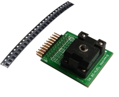
附带插座适配器的 GreenPAK SLG46620 (STQFN-20) 开发套件
SLG46620V-SKT 是一款插座适配器套件,可与 SLG4DVKADV GreenPAK™ Advanced 开发板或 SLG4DVKLITE GreenPAK Lite 开发板配合使用。 SLG46620V-SKT 套件包含 SLG4SA20-20x30 插座适配器和 50 个 SLG46620V (STQFN-20) GreenPAK 可编程混合信号矩阵 IC 样品。
GreenPAK 高级开发板和 Lite 开发板与 SLG46xxxX-SKT 和 SLG47xxxV-SKT 插座套件配合使用,为 GreenPAK 器件提供完整的编程、仿真和测试功能。
SLG46620... 阅读详情
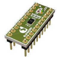
GreenPAK SLG46620 (STQFN-20) 20 引脚 DIP 原型开发板
SLG46620V-DIP 20 引脚 DIP 原型开发板非常适合用于借助 SLG46620 可编程混合信号矩阵 IC 进行的模拟板试验和快速原型开发。 该板需要 SLG4SA-DIP DIP 适配器才能与 GreenPAK™ Advanced 开发板配合使用。
GreenPAK DIP 适配器是一种小型 PCB,可将 STQFN 封装调整为 DIP 引脚布局。 这款 0.43 英寸 x 1.03 英寸的小型电路板使用 20 引脚 DIP 引脚布局,宽度为 0.3 英寸。 通过使 STQFN 封装与无焊料模拟板兼容,用户还可将此适配器用于原型开发。
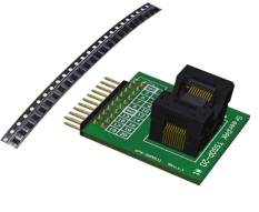
带插座适配器的 GreenPAK SLG46620 (TSSOP-20) 开发套件
SLG46620G-SKT 是一款插座适配器套件,可与 SLG4DVKADV GreenPAK™ Advanced 开发板或 SLG4DVKLITE GreenPAK Lite 开发板配合使用。 SLG46620G-SKT 套件包含 SLG4SA20-65x64 插座适配器和 50 个 SLG46620G (TSSOP-20) GreenPAK 可编程混合信号矩阵 IC 样品。
GreenPAK 高级开发板和 Lite 开发板与 SLG46xxxX-SKT 和 SLG47xxxV-SKT 插座套件配合使用,为 GreenPAK 器件提供完整的编程、仿真和测试功能。
SLG46620... 阅读详情
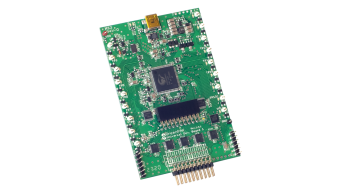
GreenPAK 高级开发板
GreenPAK™ 高级开发板为 GreenPAK 器件提供完整的编程、仿真和测试功能 - 适用于 SLG46xxxX-SKT / SLG47xxxV-SKT 插座套件。
它与 GreenPAK Designer 软件(内置于 Go Configure™ Software Hub 中)协同工作,并允许设计人员: 快速对自定义样品进行编程、 在线测试GreenPAK项目、 和使用任 一 GreenPAK 器件进行开发。
请注意:插座适配器应单独订购
远程测试该板卡
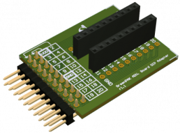
用于 GreenPAK 高级开发板的 GreenPAK DIP 适配器
借助用于 GreenPAK™ 高级开发板的 GreenPAK DIP 适配器,可以将 SLG46xxxV-DIP 和 SLG47xxxV-DIP 原型开发板与 GreenPAK 高级开发板配合使用。 此器件是高级开发平台和 DIP 开发平台之间的桥梁。
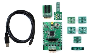
GreenPAK 入门套件
SLG4DVKINTRO GreenPAK™ 入门套件是客户开始新开发项目的理想起点。 此综合套件包含 SLG4DVKADV GreenPAK 高级开发板和 SLG4SA-DIP 适配器,后者可与开发板无缝配合使用。 此外,该套件还包含一系列 DIP 原型板:SLG46120V-DIP、SLG46721V-DIP、SLG46620V-DIP、SLG46537V-DIP 和 SLG46826V-DIP 各两块,以及 SLG47105V-DIP 和 SLG47004V-DIP 各一块。 此外,还随附一条 USB 电缆,用于实现开发过程中的连接和简化操作。
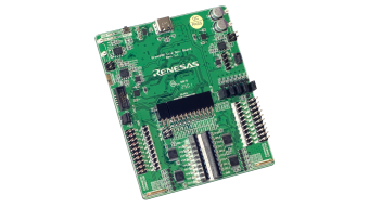
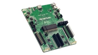
GreenPAK Lite 开发板
GreenPAK Lite 开发板为 GreenPAK 设备提供完整的编程、仿真和测试功能,与 Go Configure™ 软件中心配对工作。 板卡功能由瑞萨电子的 RX66T MCU 提供。
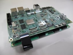
RZ/V2H 四核视觉 AI MPU 评测套件
RZ/V2H AI MPU 评测套件 (RTK0EF0168C04000BJ) 用于评测瑞萨电子 RZ/V2H 四核视觉 AI MPU。 该套件包括 CPU 板和扩展 (EXP) 板。 支持 RZ/V2H 标准软件包,能轻松实现低功耗 AI 推理和视频流等软件开发任务。 此外,这款评测套件还支持图像信号处理器 (ISP)、3D 图形引擎 (GE3D) 和可信安全 IP 等可选功能。
远程测试该板卡
GreenPAK 入门套件 Lite
SLG4DVKLITEINTRO 套件是一款一体化开发套件,专为使用 GreenPAK™ 可编程混合信号 IC 开始新项目的工程师和开发人员设计。 该套件包含带有 USB 电缆的 SLG4DVKLITE Lite 开发板和十个 DIP 原型板(SLG46120V-DIP、SLG46721V-DIP、SLG46620V-DIP、SLG46537V-DIP、SLG46826V-DIP、SLG47105V-DIP、SLG47004V-DIP、SLG47003V-DIP、SLG47011V-DIP、SLG46855V-DIP)。
此套件非常适合用于借助各种 GreenPAK 器件进行的快速评估... 阅读详情
Partner Boards & Kits
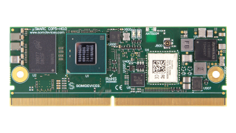
Banana PI BPI-AI2H System on Module (SoM)
Banana Pi BPI-AI2N System on Module (SoM) & BPI-AI2N Carrier